
Elastic properties and Ion-mediated domain switching of self-assembled heterostructures CuInP2S6-In4/3P2S6

 , ...
, ... Abstract
Van der Waals (vdW) ferroelectric CuInP2S6 (CIPS) has attracted intense research interest due to its unique ferroelectric properties that make it promising for potential applications in flexible electronic devices. A mechanical mean, or so-called strain gradient engineering, has been proven as an effective method to modulate its ferroelectric properties, but the key parameter elastic constants Cij has not been accurately measured. Here, we utilized nanoindentation and contact resonance atomic force microscopy (CR-AFM) techniques to measure the elastic modulus on the (001) plane of nanoscale phase separated CuInP2S6-In4/3P2S6 (CIPS-IPS). The Young’s modulus of the CIPS was slightly less than that of the IPS. Density Functional Theory was introduced to obtain the accurate full elastic constant Cij of CIPS and IPS, and we deduced their respective Young’s moduli, all of which are in good agreement with our experimental values. We further discovered the asymmetrical domain switching and proposed an ion-mediated domain switching model. The results provide a reliable experimental reference for strain gradient engineering in the phase field simulation in CIPS-IPS.
Keywords
INTRODUCTION
Van der Waals layered ferroelectric CuInP2S6 (CIPS) has attracted intense research interest due to its unique ferroelectric characteristics. A series of novel properties have been discovered in recent years, such as giant negative piezoelectricity[1], tunable quadruple energy wells[2], large room temperature electrocaloric effect[3,4], and strong coupling between ferroelectric polarization and ionic conductivity[5-7]. Based on these fascinating attributes, large quantities of 2D device applications have shown up in the past several years, including ferroelectric field-effect transistors[8-10], ferroelectric tunneling junctions[11], negative capacitance field-effect transistors[12,13], memristors[5,14] and prototype neuromorphic computing[15-18].
The crystal structure of CIPS can be described as a sulfur framework in which metal cations (Cu and In) and P-P pairs fill the octahedral voids[19]. It is noteworthy that when Cu is deficient, the system undergoes a chemical phase separation into a paraelectric IPS phase and a ferroelectric CIPS phase[20,21] due to the intentionally induced off-stoichiometry. Compared with normal CIPS, CIPS-IPS has a higher Curie temperature (340 K > 315 K)[21-23], a tunable dielectric property[24] and a porous structure in which the IPS phase is more conducive to the lateral migration of Cu ions[6,19]. In addition, the ferroelectric properties of CIPS-IPS have sensitive response to out-of-plane mechanical stimuli[7]. Recently, the utilization of strain engineering to modulate the domain and phase has become a promising method[25,26]. However, there is a lack of key parameters such as elastic coefficient to give accurate reference for the experimental and theoretical investigation of this system[27,28].
In this work, we use a combination of contact resonance atomic force microscopy and piezoresponse force microscopy (CR-AFM and PFM) to achieve accurate Young’s modulus of CIPS and IPS in the nanoscale phase separated CIPS-IPS. The results reveal that the Young’s modulus of the CIPS phase was
METHODS
Sample preparation and structure characterization
We synthesized CuxInyP2S6 single crystal through the chemical vapor transport method[20]. The starting materials were sealed in fused silica ampules, then heated to 750-775 °C at a rate of 30 °C/h and held at that temperature for 4 days, followed by a rate of 20 °C/h cooling. The thin flakes were obtained by mechanical exfoliation and transferred to the conductive Au/SiO2/Si substrate. The energy dispersive spectroscopy (EDS) was performed using a commercial ultra-high resolution cold-field emission scanning electron microscopy system (Hitachi, Regulus 8230) to characterize the elemental compositions. The actual chemical composition was determined to be Cu0.57In1.04P2S6.
DFT calculations
The density functional theory (DFT) calculation was carried out using the projector augmented wave (PAW)[30] scheme with the Perdew-Burke-Ernzerhof (PBE) functional of generalized gradient approximation (GGA)[31] method as implemented in the Vienna ab initio simulation package (VASP)[32,33]. A plane wave cutoff of 450 eV was set in our calculations. K-point samplings of 5 × 3 × 2 were used. DFT-D3(BJ) level[34,35] was used in our calculations to take into consideration of the van der Waal forces. Atomic relaxation was performed until the force on each atom was smaller than 0.001 eV Å-1, and the total energy change was less than 10-6 eV. The space group of CuInP2S6 and In4/3P2S6 are Cc and P21/c, respectively. The unit cell CuInP2S6 contains 4 Cu, 4 In, 8 P and 24 S atoms, while the In4/3P2S6 contains 8 In, 12 P and 36 S atoms. The calculated lattice parameters are listed in Supplementary Table 1, which are consistent with previously reported experimental values[36,37].
Scanning probe microscopy
Piezoresponse force microscopy (PFM) and conductive-atomic force microscopy (c-AFM) measurements were performed using a commercial atomic force microscope (Asylum Research MFP-3D) with Pt/Ir-coated Si cantilever tips (radius of ~25 nm). The spring constant is in the range of ~0.5-9.5 N/m. The out-of-plane (OP) phase and amplitude images were acquired using the dual-frequency resonance tracking piezoresponse force microscopy (DART-PFM) mode with an ac voltage (Vac = 2 V). The conductive Si cantilever was excited with an ac voltage of 2 V at the tip-sample contact resonant frequency of ~350 kHz. The switching spectroscopy PFM (SS-PFM) was performed to obtain the hysteresis loops to characterize the local ferroelectricity. In c-AFM measurement, the voltage was applied to the conducting Au bottom electrode, which was continuously swept and simultaneously read the current. In contact resonance atomic force microscopy (CR-AFM) measurement, the NCL Pt-coated tips with k ≈ 48 N/m were used. The contact force between the cantilever and the sample was ~25 µN. More calculation details of Young’s modulus are presented in the Supplementary Information.
Raman measurement
Raman spectra were collected using a micro-Raman system with a Horiba iHR550 spectrometer and a 100X objective (Olympus, NA = 0.95). A 633 nm Helium-Neon Laser (Newport) was used to excite the Raman scattering and the laser power was low enough to avoid excessive heating of the sample. Raman measurements were performed under a microscope in backscattering configuration with linear polarized excitation and unpolarized detection.
Nanoindentation measurement
The nanoindentation experiments were performed using a commercial nanoindenter (G200 Keysight), which has load and displacement resolutions of 50 nN and 0.01 nm, respectively. The indentation tests were conducted normal to the (001) plane at room temperature with a Berkovich indenter. Calibration was performed using fused silica with a modulus of 72.1 GPa. The sample was fixed to the silicon wafer by the commercially provided mounting glue. Then the glue and sample were cured for at least 24 h.
RESULTS AND DISCUSSION
The CIPS-IPS crystal has millimeter-sized lateral dimension and a thickness of ~tens micrometers, as shown in Figure 1A. The crystal is transparent and flexible. For the subsequent structural characterization, thin flakes of CIPS-IPS were prepared by mechanical exfoliation, as shown in the bottom panel of Figure 1A. Figure 1B shows the crystal structure of IPS, CIPS and CIPS-IPS heterostructure. IPS is non-polar due to a lack of Cu ions. To confirm that this sample is indeed a two-phase coexisted CIPS-IPS crystal, we compare the Raman spectrum with that of CIPS crystal, as shown in Figure 1C. Two peaks appear at ~255 and
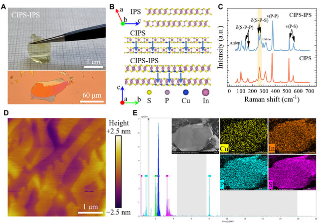
Figure 1. Structural and chemical characterizations. (A) a CIPS-IPS crystal (up) and nano flakes on conductive Au/SiO2/Si substrates(down). (B) crystal structure of IPS (viewed along the b-axis), CIPS and CIPS-IPS heterostructure (viewed along the a-axis), respectively. The blue arrows represent the direction of polarization. (C) Raman spectra of CIPS-IPS and IPS flakes. (D) a representative surface topography of CIPS-IPS nano flake measured by AFM. (E) a representative energy-dispersive x-ray spectrum of the CIPS-IPS crystal. The inset shows the SEM image and corresponding elemental mappings.
To accurately measure the Young’s modulus (Es) of the (001) plane of the crystal, three independent quasi-static nanoindentation tests were performed. The indentation depth was kept well below 1/10 of the total thickness of the single crystal. The peak loading was set as 16 mN with the purpose of obtaining the depth-independent elastic modulus, and the loading/unloading rates were set as 0.25 mN/s. To minimize the influence of time-dependent plastic effects and obtain entirely elastic unloading curves, the peak loading was maintained for 10 s before unloading. All nanoindentation P-h curves are shown in Figure 2A. We can see a few pop-ins which are caused by fracture or dislocation[38]. The reduced modulus can then be deduced from the slope of load-displacement curve, dP/dh, upon unloading, using the following Oliver-Phar model[39]:

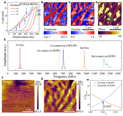
Figure 2. Elastic property characterizations. (A) Nanoindentation Load–displacement curves measured on the (001) plane of CIPS-IPS crystal. The blue arrows indicate pop-ins due to fracture damage. (B) The contact resonant frequency image measured by CR-AFM.
where Er is the reduced Young’s modulus, β is the geometry constant close to unity (1.058 for Berkovich indenter), and A is the projected area of the indentation at the contact depth hc. For a Berkovich tip,  24.5 hc2.

where EI is the elastic modulus of the indenter (1140 GPa for diamond), vs and vI are the Poisson’s ratios of the sample and the indenter. The Poisson’s ratio of diamond is 0.07 and that of CIPS-IPS is close to zero. The Es of CIPS-IPS is calculated to be around 22.20 ± 0.48 GPa.
A critical issue is that we do not know whether the nanoindentation position is CIPS or IPS. To further correlate it with the corresponding regions, we characterize the same regions with the aid of CR-AFM, Lateral Force Microscopy (LFM), and PFM. Figure 2B-D show resonance frequency, friction force and phase images, respectively. The corresponding complete PFM amplitude and deflection images are shown in Supplementary Figure 2. The frequency and friction force images corresponding to the CIPS phase and IPS show a labyrinth-like distribution which can also be seen from the frequency statistics curve in Supplementary Figure 3. In addition, the CIPS phase resonance frequency is larger, and the corresponding friction force is smaller. This phenomenon can be understood as follows: the higher the resonance frequency, the higher the Young’s modulus, which is simply the harder. When measuring the lateral force under the same pressure, the friction force of the harder material is smaller if ignoring other interface factors, which is consistent with our experimental observation. Note that the direction of polarization has little effect on the magnitude of the modulus and the magnitude of the frictional force. In addition, we also ruled out the influence of topography fluctuation itself on the friction measurement; the magnitude of the friction is still continuous, even if in the two regions of the fault [Supplementary Figure 4].
In order to quantify the magnitude of elastic modulus of different phases of CIPS-IPS, a reference material of highly oriented pyrolytic graphite (HOPG) with a modulus of 15 GPa[40] was used for calibration, given the difficulty in accurately determining the tip radius and contact area. Typical first and second-order contact resonance frequency (CRF) spectra are shown in Figure 2E, from which the higher CRF of CIPS reflects its higher modulus. The relative tip position γ was determined as 0.92 from the intersection of curves for the first and second modes of HOPG [Figure 2H]. Then, the mappings of the first-order CRF were also carried out in HOPG and CIPS-IPS, as shown in Figure 2F and G. By fitting the resonance frequency-frequency distribution curves of Figure 2F and G inset, the mean value and deviation of the resonance frequency were obtained. In order to more accurately determine the value of elastic modulus, single-point measurements of the contact resonance frequency were performed on the basis of the modulus mapping image, and the results are shown in Supplementary Table 3.
The process of the contact resonance model to quantify Young’s modulus is as follows:
When the cantilever vibrates freely in the air, according to the cantilever flexural vibration governing equation and boundary conditions, the characteristic equation can be obtained:

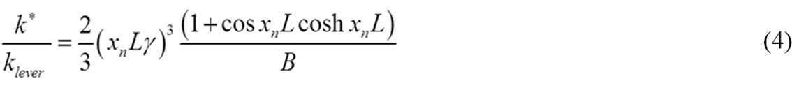
The first two roots of Equation (3) are [x10L, x20L,] = [1.8751,4.6941][41,42]. When the cantilever tip is in contact with the sample, the normalized contact stiffness k*/klever can be expressed as the nth order flexural contact resonance and the relative tip position γ as[41]:
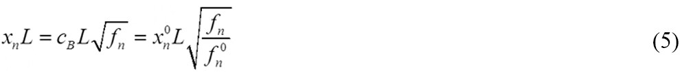
where k* and klever are the contact stiffness and the spring constant of the cantilever, respectively. γ is the relative position of the tip at the end of the cantilever. The values of flexural resonance wavenumber xnL can be calculated with the nth order resonant frequency fn of the tip-sample system[41]:
Therefore, the cantilever parameter cBL for each mode can be obtained directly from the free resonance frequencies fn0. Because the normalized contact stiffness of the first and second modes k*/klever should be the same, the relative tip position γ can be determined by the intersection of the two modes k*/klever-γ curves plotted from Equation (4), as shown in Figure 2H. On this basis, the reduced modulus Es* of the sample can be calculated from the normalized contact stiffness k*/klever as:
where Eref* is the reduced modulus of reference material, and can be obtained from Equation (2). ks*/klever and kref*/klever are the normalized contact stiffness of sample and reference material, respectively. Then, the elastic modulus Es of the sample can be calculated from the reduced modulus Es* using Equation (2).
Combined with the Equations (2 and 4-6), the elastic modulus of CIPS-IPS was calculated and the results are listed in Table 1. It is worth noting that the Poisson’s ratio used in the actual calculation comes from the result obtained from the conversion of the elastic coefficient calculated by DFT. The Poisson’s ratio of CIPS is -0.044 (the value of the reference is -0.060[43]), and the Poisson’s ratio of IPS is 0.107, as shown in Table 1. The elastic modulus of CIPS phase is 27.42 ± 0.05 GPa, which is slightly smaller than that of IPS phase, which is 27.51 ± 0.04 GPa. The moduli obtained by the CR-AFM measurement of both CIPS and IPS are larger than the Young’s modulus result of 22.20 ± 0.48 GPa from the nanoindentation measurement. This may be induced by the fractures or the effect of dislocations during the indenting process. Through the results of the continuous stiffness method [Supplementary Figure 5], we can find that the modulus gradually decreases with the increase of the indentation depth, which confirms the effect of fracture in reducing the measured modulus value of nanoindentation measurement.
Elastic modulus of CIPS and IPS by CR-AFM
| Properties | Tip Si | HOPG | CIPS | IPS |
| 1st CRF (kHz) | 653.01 ± 0.25 | 695.81 ± 0.11 | 696.15 ± 0.08 | |
| Ez (GPa) | 160 | 15 | 27.42 ± 0.05 | 27.51 ± 0.04 |
| v (Poisson’s ratio) | 0.28 | 0.2 | -0.044 | 0.107 |
In order to confirm the difference in the elastic modulus of the two phases, we used density functional theory (DFT) to accurately calculate the elastic matrices of the CIPS phase and the IPS phase (The crystal structure parameters of CIPS and IPS are listed in Supplementary Table 1), and the results are shown in Table 2. From the table, we can find that the modulus of IPS is larger than that of CIPS, with a difference of nearly 1.23 GPa, which is consistent with our experimental results.
Elastic properties of CIPS and IPS by DFT
| Properties (GPa) | C11 | C22 | C33 | C23 | C13 | C12 | C44 | C55 | C66 | C15 | C25 | C35 | C64 | Ez |
| CIPS | 99.86 | 101.68 | 28.02 | -3.85 | -4.71 | 25.49 | 6.99 | 6.71 | 37.56 | 1.93 | 4.10 | 2.55 | 0.91 | 26.57 |
| IPS | 89.07 | 75.74 | 33.27 | 9.72 | 10.03 | 23.12 | 25.96 | 11.67 | 9.90 | -6.86 | -13.56 | 3.77 | -8.33 | 27.80 |
To further study the ferroelectric property of CIPS-IPS, the flakes were obtained by mechanical exfoliation and then transferred to Au-coated silicon. Figure 3A shows the topography, which indicates the thickness is around 176.2 nm. The corresponding phase image is shown in Figure 3B, and the enlarged amplitude and phase signals of blue-boxed region are shown in Figure 3D and E, respectively. The vanish of amplitude signal indicates the region of non-ferroelectric IPS phase. In contrast, there are two opposite polarization states in the CIPS phase, such as the yellow domain (point P1) and the black domain (point P2). There are three phase state distribution characteristics, in which the intermediate contrast is from non-polarized IPS. We also found this common phenomenon in other regions and performed statistical analysis on its area distribution, and the results are shown in Supplementary Figure 6. In addition, we measured the ferroelectric hysteresis curves of the two domains of CIPS phase, and the results are shown in Figure 3C-F. We can clearly see that the phases and amplitudes of both domains exhibit typical characteristics of ferroelectric materials. It is worth mentioning that the hysteresis curves of different domains deviate from the 0 V, which is mainly caused by the difference in the depolarization fields. Based on the amplitude-voltage curves, we calculated the equivalent piezoelectric coefficient d33 of the CIPS phase, and the value of
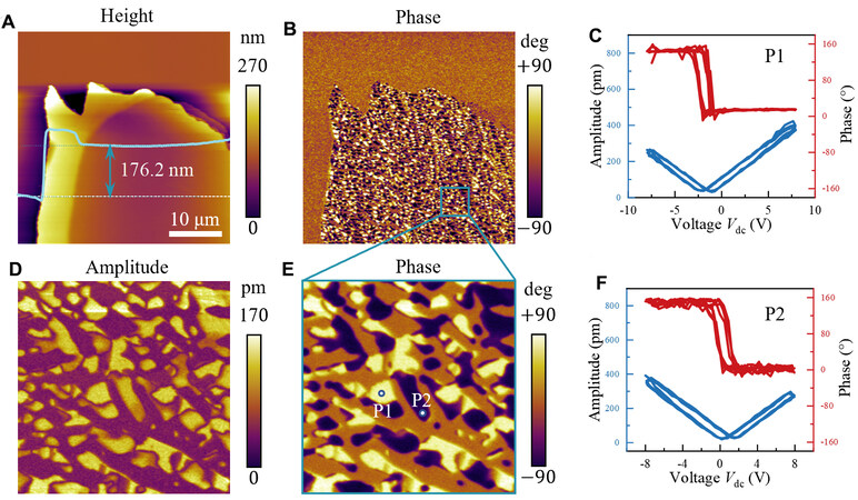
Figure 3. Ferroelectric characterizations of CIPS-IPS crystal. (A and B): a representative topography and phase images. Inset: height curve at white section line. (C and F): the PFM phase and amplitude hysteresis loops in P1 (polarization downward) and P2 (polarization upward), respectively. (D and E): the enlarged amplitude and phase images in the blue boxed region of (B).
The polarization direction is determined by switching domains in random regions, and the results are shown in Figure 4A and B. The voltage of writing domain is shown in the inset, -6 V for the upper 1/3 area and +6 V for the lower 2/3 area. As a result, most of the yellow domains in the upper 1/3 area were switched into black domains, while the lower 2/3 area did not change significantly. Thus, the yellow (black) domains represent the downward (upward) polarization. To further confirm this speculation, we continued to write domains in the same region with -6 V voltage, and the results are shown in Figure 4C. We can clearly find that most of the yellow domain switch to black domain, while the original non-polarization IPS phase and black domains do not change significantly. This again confirms that the black domain corresponds to upward polarization. We then applied a +6 V voltage at the same region, and the result is shown in Figure 4D. The entire domain did not change, and the amplitude signal of the PFM was weakened. The mean value was only 2/3 of the original amplitude in the CIPS phase. This means that a voltage of +6 V is not able to switch the polarization or even reduce its piezoelectric response. Note that Figure 4A-D are modified images by clustering method to facilitate readers to see the changes in domain structure clearly. The original images are shown in Supplementary Figure 8.
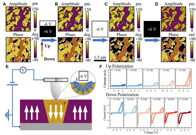
Figure 4. Domain switching and ionic migration characterizations of CIPS-IPS crystal. (A-D) The amplitude and phase images of initial, after applying -6 V/+6 V bias, after applying -6 V bias and after applying +6 V bias, respectively. The scale bar is 1.5 μm. (E) Schematic diagram of ion migration in CIPS under tip electric field. Red balls represent copper ions. The white and blue arrows indicate the polarization direction and the electric field direction, respectively. (F) Current-voltage(I-V) curves at different scan rates in different polarization areas.
To explain this interesting phenomenon, we refer to previous studies on ion migration in CIPS and propose a model of ion migration-mediated nonreciprocal domain switching, as shown in Figure 4E. In the schematic diagram, red balls represent Cu ions. When a voltage of tip bias -6 V is applied to the sample surface, the electric field converges towards the probe tip, as the inset indicates. The Cu ions migrate to the probe and decrease the Schottky barrier between the probe and the sample. The effective electric field directly acting on the CIPS phase is enough to switch the domain, and the yellow domain is switched to the black domain. On the contrary, when a voltage of +6 V is applied, the direction of the electric field diverges from the probe, and the Cu ions are driven away from the tip, and the effective electric field acting on the CIPS phase therefore cannot switch domain. As a result, all domains did not change significantly, and the overall piezoelectric response decreased. To confirm ion mobility in CIPS-IPS, we characterized the macroscopically manifested I-V curves, and the results are shown in Figure 4F. In the upward polarization region, we can find that the forward current gradually increases as the rate of the applied bias cycle decreases. Likewise, in the downward polarization region, the forward current is also large at lower voltage sweep speeds. Nevertheless, with the increase of scanning speed, the whole forward current decreases until zero, while the reverse current gradually increases and tends to be stable. All suggest that Cu ion migration dominates the current feature, which is consistent with our previous studies on current regulation in pure CIPS[16]. These results favorably confirm that Cu ions mediate the switching of ferroelectric domains.
CONCLUSIONS
In conclusion, we accurately characterized the Young’s modulus of the CIPS-IPS two phases for the first time by various experimental methods (nanoindentation method and atomic force contact resonance method) in this study, and the Young’s modulus of the CIPS phase was 27.42 ± 0.05 GPa, slightly less than that of the IPS phase, which was 27.51 ± 0.04 GPa. In addition, we calculated the elastic matrices of the two phases of CIPS-IPS using the first-principles method, and deduced their respective Young’s modulus, all of which are in good agreement with our experimental values. Finally, we also discover the asymmetry of domain switching and propose an ion-mediated nonreciprocal domain switching model, which strongly explains this interesting phenomenon. Our work provides a reliable experimental reference for the follow-up study of the elastic properties of CIPS-IPS and the phase field simulation for regulating the domain structure.
DECLARATIONS
Authors’ contributionsAFM characterization, writing original draft: Zhang X
Review & editing, supervision: Jiang X
Raman characterization: Du G
DFT calculation: Ren Q
EDS characterization: Zhu W
Sample synthesis: Kang J, Deng J
Guidance for experiment and data analysis: Lun Y, Wang T, Bai B, Yu Z
Conceptualization, review, supervision: Hong J, Wang X, Chen Y
Availability of data and materialsThe list of elemental atomic percentages of different CIPS flakes obtained from EDS, single-point CRF measurement results of CIPS-IPS and HOPG by CR-AFM, CR-AFM method, A: frequency and friction histogram and original PFM data are provided in Supplementary Information.
Financial support and sponsorshipThe work at Beijing Institute of Technology is supported by National Natural Science Foundation of China with Grant Nos. 12172047, 11604011, 92163101, 12202056, National Key Research and Development Program of China (2019YFA0307900), the Beijing Natural Science Foundation (Z190011), and Beijing Institute of Technology Research Fund Program for Young Scholars.
Conflicts of interestAll authors declared that there are no conflicts of interest.
Ethical approval and consent to participateNot applicable.
Consent to publicationNot applicable.
Copyright© The Author(s) 2023.
Supplementary MaterialsREFERENCES
1. You L, Zhang Y, Zhou S, et al. Origin of giant negative piezoelectricity in a layered van der Waals ferroelectric. Sci Adv 2019;5:eaav3780.
2. Brehm JA, Neumayer SM, Tao L, et al. Tunable quadruple-well ferroelectric van der Waals crystals. Nat Mater 2020;19:43-8.
3. Niu L, Liu F, Zeng Q, et al. Controlled synthesis and room-temperature pyroelectricity of CuInP2S6 ultrathin flakes. Nano Energy 2019;58:596-603.
4. Si M, Saha AK, Liao PY, et al. Room-temperature electrocaloric effect in layered ferroelectric CuInP2S6 for solid-state refrigeration. ACS Nano 2019;13:8760-5.
5. Zhou S, You L, Chaturvedi A, et al. Anomalous polarization switching and permanent retention in a ferroelectric ionic conductor. Mater Horiz 2020;7:263-74.
6. Xu D, Ma R, Zhao Y, et al. Unconventional out-of-plane domain inversion via in-plane ionic migration in a van der Waals ferroelectric. J Mater Chem C 2020;8:6966-71.
7. Neumayer SM, Brehm JA, Tao L, et al. Local strain and polarization mapping in ferrielectric materials. ACS Appl Mater Interfaces 2020;12:38546-53.
8. Si M, Liao PY, Qiu G, Duan Y, Ye PD. Ferroelectric field-effect transistors based on MoS2 and CuInP2S6 two-dimensional van der waals heterostructure. ACS Nano 2018;12:6700-5.
9. Huang W, Wang F, Yin L, et al. Gate-coupling-enabled robust hysteresis for nonvolatile memory and programmable rectifier in van der waals ferroelectric heterojunctions. Adv Mater 2020;32:e1908040.
10. Singh P, Baek S, Yoo HH, Niu J, Park JH, Lee S. Two-dimensional CIPS-InSe van der Waal heterostructure ferroelectric field effect transistor for nonvolatile memory applications. ACS Nano 2022;16:5418-26.
11. Liu F, You L, Seyler KL, et al. Room-temperature ferroelectricity in CuInP2S6 ultrathin flakes. Nat Commun 2016;7:12357.
12. Wang X, Yu P, Lei Z, et al. Van der Waals negative capacitance transistors. Nat Commun 2019;10:3037.
13. Neumayer SM, Tao L, O’hara A, et al. The concept of negative capacitance in ionically conductive van der Waals ferroelectrics. Adv Energy Mater 2020;10:2001726.
14. Li B, Li S, Wang H, et al. An electronic synapse based on 2D ferroelectric CuInP2S6. Adv Electron Mater 2020;6:2000760.
15. Yue K, Liu Y, Lake RK, Parker AC. A brain-plausible neuromorphic on-the-fly learning system implemented with magnetic domain wall analog memristors. Sci Adv 2019;5:eaau8170.
16. Jiang X, Wang X, Wang X, et al. Manipulation of current rectification in van der Waals ferroionic CuInP2S6. Nat Commun 2022;13:574.
17. Chen J, Zhu C, Cao G, et al. Mimicking neuroplasticity via ion migration in van der waals layered copper indium thiophosphate. Adv Mater 2022;34:e2104676.
18. Guo R, Zhou Y, Wu L, et al. Control of synaptic plasticity learning of ferroelectric tunnel memristor by nanoscale interface engineering. ACS Appl Mater Interfaces 2018;10:12862-9.
19. Zhang D, Luo ZD, Yao Y, et al. Anisotropic ion migration and electronic conduction in van der Waals ferroelectric CuInP2S6. Nano Lett 2021;21:995-1002.
20. Susner MA, Belianinov A, Borisevich A, et al. High-Tc layered ferrielectric crystals by coherent spinodal decomposition. ACS Nano 2015;9:12365-73.
21. Susner MA, Chyasnavichyus M, Puretzky AA, et al. Cation-eutectic transition via sublattice melting in CuInP2S6-In4/3P2S6 van der Waals layered crystals. ACS Nano 2017;11:7060-73.
22. Rao R, Selhorst R, Conner BS, Susner MA. Ferrielectric-paraelectric phase transitions in layered CuInP2S6 and CuInP2S6-In4/3P2S6 heterostructures: a Raman spectroscopy and x-ray diffraction study. Phys Rev Mater 2022; 6:045001.
23. Checa M, Ivanov I, Neumayer SM, et al. Correlative piezoresponse and micro-Raman imaging of CuInP2S6-In4/3P2S6 flakes unravels phase-specific phononic fingerprint via unsupervised learning. Appl Phys Lett 2022;121:062901.
24. Neumayer SM, Eliseev EA, Susner MA, et al. Giant negative electrostriction and dielectric tunability in a van der Waals layered ferroelectric. Phys Rev Mater 2019;3:024401.
25. Chen C, Liu H, Lai Q, et al. Large-scale domain engineering in two-dimensional ferroelectric CuInP2S6 via giant flexoelectric effect. Nano Lett 2022;22:3275-82.
26. Rao R, Conner BS, Selhorst R, Susner MA. Pressure-driven phase transformations and phase segregation in ferrielectric
27. Ming W, Huang B, Zheng S, et al. Flexoelectric engineering of van der Waals ferroelectric CuInP2S6. Sci Adv 2022;8:eabq1232.
28. Eliseev EA, Fomichоv YM, Kalinin SV, Vysochanskii YM, Maksymovich P, Morozovska AN. Labyrinthine domains in ferroelectric nanoparticles: manifestation of a gradient-induced morphological transition. Phys Rev B 2018;98:054101.
29. Checa M, Jin X, Millan-Solsona R, et al. Revealing fast cu-ion transport and enhanced conductivity at the CuInP2S6-In4/3P2S6 heterointerface. ACS Nano 2022;16:15347-57.
30. Blöchl PE, Jepsen O, Andersen OK. Improved tetrahedron method for Brillouin-zone integrations. Phys Rev B Condens Matter 1994;49:16223-33.
31. Perdew JP, Burke K, Ernzerhof M. Generalized gradient approximation made simple. Phys Rev Lett 1996;77:3865-8.
32. Kresse G, Furthmüller J. Efficient iterative schemes for ab initio total-energy calculations using a plane-wave basis set. Phys Rev B 1996;54:11169-86.
33. Kresse G, Furthmüller J. Efficiency of ab-initio total energy calculations for metals and semiconductors using a plane-wave basis set. Comput Mater Sci 1996;6:15-50.
34. Grimme S, Antony J, Ehrlich S, Krieg H. A consistent and accurate ab initio parametrization of density functional dispersion correction (DFT-D) for the 94 elements H-Pu. J Chem Phys 2010;132:154104.
35. Grimme S, Ehrlich S, Goerigk L. Effect of the damping function in dispersion corrected density functional theory. J Comput Chem 2011;32:1456-65.
36. Maisonneuve V, Evain M, Payen C, Cajipe V, Molinié P. Room-temperature crystal structure of the layered phase CuInP2S6. J Alloys Compd 1995;218:157-64.
37. Diehl R, Carpentier C. The structural chemistry of indium phosphorus chalcogenides. Acta Crystallogr B Struct Sci 1978;34:1097-105.
38. Fang X, Bishara H, Ding K, et al. Nanoindentation pop-in in oxides at room temperature: dislocation activation or crack formation? J Am Ceram Soc 2021;104:4728-41.
39. Oliver W, Pharr G. An improved technique for determining hardness and elastic modulus using load and displacement sensing indentation experiments. J Mater Res 1992;7:1564-83.
40. Xiao J, Zhang L, Zhou K, Li J, Xie X, Li Z. Anisotropic friction behaviour of highly oriented pyrolytic graphite. Carbon 2013;65:53-62.
41. Zhu Q, Pan K, Xie S, Liu Y, Li J. Nanomechanics of multiferroic composite nanofibers via local excitation piezoresponse force microscopy. J Mech Phys Solids 2019;126:76-86.
42. Hurley DC. Contact resonance force microscopy techniques for nanomechanical measurements. In Applied scanning probe methods XI. Heidelberg, Berlin: Springer, 2009; pp. 97-138.
43. Zhang C, Nie Y, Du A. Intrinsic ultrahigh negative Poisson’s ratio in two-dimensional ferroelectric ABP2x6 materials. Acta Physico-Chimica Sinica 2019;35:1128-33.
Cite This Article
Export citation file: BibTeX | RIS
OAE Style
Zhang X, Jiang X, Du G, Ren Q, Zhu W, Kang J, Lun Y, Wang T, Bai B, Yu Z, Deng J, Chen Y, Wang X, Hong J. Elastic properties and Ion-mediated domain switching of self-assembled heterostructures CuInP2S6-In4/3P2S6. Microstructures 2023;3:2023010. http://dx.doi.org/10.20517/microstructures.2022.39
AMA Style
Zhang X, Jiang X, Du G, Ren Q, Zhu W, Kang J, Lun Y, Wang T, Bai B, Yu Z, Deng J, Chen Y, Wang X, Hong J. Elastic properties and Ion-mediated domain switching of self-assembled heterostructures CuInP2S6-In4/3P2S6. Microstructures. 2023; 3(2): 2023010. http://dx.doi.org/10.20517/microstructures.2022.39
Chicago/Turabian Style
Zhang, Xiangping, Xingan Jiang, Guoshuai Du, Qi Ren, Wenfu Zhu, Jiaqian Kang, Yingzhuo Lun, Tingjun Wang, Bofang Bai, Zixuan Yu, Jianming Deng, Yabin Chen, Xueyun Wang, Jiawang Hong. 2023. "Elastic properties and Ion-mediated domain switching of self-assembled heterostructures CuInP2S6-In4/3P2S6" Microstructures. 3, no.2: 2023010. http://dx.doi.org/10.20517/microstructures.2022.39
ACS Style
Zhang, X.; Jiang X.; Du G.; Ren Q.; Zhu W.; Kang J.; Lun Y.; Wang T.; Bai B.; Yu Z.; Deng J.; Chen Y.; Wang X.; Hong J. Elastic properties and Ion-mediated domain switching of self-assembled heterostructures CuInP2S6-In4/3P2S6. Microstructures. 2023, 3, 2023010. http://dx.doi.org/10.20517/microstructures.2022.39
About This Article
Copyright

Data & Comments
Data


 Cite This Article 16 clicks

 Like This Article 0
likes
Like This Article 0
likes


Comments
Comments must be written in English. Spam, offensive content, impersonation, and private information will not be permitted. If any comment is reported and identified as inappropriate content by OAE staff, the comment will be removed without notice. If you have any queries or need any help, please contact us at support@oaepublish.com.