
Microstructural constructing 2D tin allotropes on Al(111): from quasi-periodic lattice to square-like lattice
 0
0 , ...
, ... Abstract
The lattice arrangement and degree of buckling have been playing vital roles in the structure stability, bonding configuration, and electronic band structures of two-dimensional (2D) single-layer materials. Here, we fabricate two tin allotropes beyond honeycomb stanene by epitaxial growth method on Al(111). Sn-I phase with quasi-periodic lattice and Sn-II phase with square-like lattice have been identified by scanning tunneling microscopy. Combined with scanning tunneling spectroscopy, it is revealed that Sn-II phase with four-coordinate tin atoms exhibits enhanced decoupling effects due to their saturated bonds. In this study, the discovery of new lattice arrangements with well-defined atomic structures beyond honeycomb lattice provides an appealing approach to searching 2D elemental single layers and novel physical properties.
Keywords
INTRODUCTION
Two-dimensional (2D) tin in honeycomb lattice, also known as stanene, has attracted enormous research attention in the field of condensed matter physics as a candidate for room temperature quantum spin Hall (QSH) insulator and recently discovered topological superconductor[1-3]. The arrangement of 2D lattice and degree of buckling have been playing vital roles in the structure stability, bonding configuration, and electronic band structures of 2D tin, as exemplified by a number of epitaxially grown stanene systems, such as planar stanene on Cu(111), strained stanene on Sb(111), and stanene Au(111)[4-12]. Aiming at either pursuing superior or new physical properties, allotropes of 2D tin beyond planar and buckled honeycomb structures have been widely predicted. 2D tin with dumbbell structure and staggered layered dumbbell structure is predicted to be a stable topological insulator and topological Dirac semimetal, respectively[13,14]. Besides, 2D tetragonal tin with repeated square and octagon rings is predicted to be a node line semimetal protected by the combination of spatial inversion and time-reversal symmetries[15]. Double-layer 2D tin with a square lattice has also been proposed to be favorable for free-standing films[16]. In contrast to the intensive theoretic exploration, experimental construction of 2D allotropes beyond honeycomb and buckled honeycomb structures, however, are rarely reported for either tin or other 2D elemental single layers[17-20], which requires subtle interaction and proper lattice-matching between the substrate and the elemental layer.
In this work, two different 2D tin allotropes with quasi-periodic lattice and square-like lattice are fabricated on Al(111) by epitaxial growth method at different tin coverages. Scanning tunneling microscopy (STM) and scanning tunneling spectroscopy (STS) studies reveal their atomic structures, electronic properties, and the degree of interaction with the substrate. We find that in the sub-monolayer region, tin overlayer prefers the quasi-periodic lattice, in which three-coordinate and four-coordinate tin atoms coexist. While at 1 monolayer (ML) and above, the quasi-periodic lattice transforms to the square-like lattice with four-coordinate tin atoms, which exhibits apparently enhanced decoupling with the substrate.
MATERIALS AND METHODS
The growth of tin on Al(111) and STM measurements were carried out in the ultra-high vacuum (>1 × 10⁻¹⁰ Torr). The Al(111) single crystal with a well-polished surface was purchased from Mateck, GmbH. The Al(111) single crystal was treated in the ultra-high vacuum condition by cycles of sputtering and annealing. The process of epitaxial growth is illustrated in Figure 1A, in which Sn atoms were evaporated from a home-made crucible onto Al(111) at 293 K. The as-grown samples were then in-situ transferred to STM chamber for characterization at 77 K. During the STM and STS tests, the voltage was applied to the sample. All the STM images were acquired at constant current mode. The dI/dV measurements were acquired with a lock-in technique with a sample voltage modulation of 10 mV at 937 Hz. The STM images were analyzed using WSxM software[21].
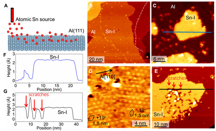
Figure 1. (A) Schematic diagram of the epitaxial growth of Sn on the surface of Al(111). (B and C) Typical scanning tunneling microscopy (STM) images of as-prepared surfaces showing the coexistence of bare substrate and sub-monolayer Sn-I phase [(2 V,
RESULTS AND DISCUSSION
Figure 1B and C show two typical surface topographies after deposition of sub-monolayer tin on Al(111) surface. The majority of islands are found on the same atomic layer of Al(111), between which an apparent boundary can be observed as indicated by the white dashed line in Figure 1B. In addition, several islands that are not adjacent to the step edges can also be found [Figure 1C]. These two types of islands turn out to show the same superstructure, as shown in Figure 1D, which exhibits hexagonal structure with a periodicity of around 1.5 nm and directions of +/- 19° with respect to Al[1
The atomic resolution STM image of Sn-I phase is shown in Figure 2A, with the unit cell of the superstructure marked by the light blue rhombus. The superstructure and lattice direction match well with the 2√7a × 2√7a R19.1° of Al(111) [shortened as 2√7a, a is the unit cell of Al(111)]. The superstructure is also apparent in the corresponding fast Fourier transform (FFT) image [Figure 2B and C], in which periodicities of 2√7a and 2√7/3a can be identified as marked by six light blue circles and six purple circles, respectively. These periodicities are reproduced in the inverse-FFT image of these spots [Figure 2D], indicating both translational and rotational symmetries of the lattice. The sketch of the 2√7a × 2√7a structure on the Al(111) substrate is exhibited in Figure 2E. It is clear that this quasi-periodicity of 2√7a is not composed by a simple triangle or honeycomb lattice, but a complex tiling of triangle, square and pentagon lattices, as mimicked in Figure 2F. From the comparison, the 2√7/3a periodicity and their surroundings satellite spots in the inverse-FFT images can be assigned to the triangle lattices with different directions as marked in Figure 2F. In addition, a set of twelve-fold spots (green circles) can be identified in the FFT image and the corresponding inverse-FFT image [Figure 2D], which forms a dodecagon lattice. This complex superstructure of Sn-I phase can be understood as a mix of three-coordinate and four-coordinate Sn atoms in the tiling of triangle, square, and pentagon units.
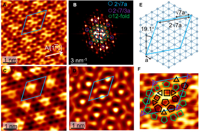
Figure 2. (A) Atomic resolution STM image of Sn-I phase with the unit cell marked by the rhombus (-50 mV, 50 pA). (B) Fast Fourier transform (FFT) image of (A) with the periodicity of 2√7a × 2√7a structure, 2√7/3a × 2√7/3a structure, and the dodecagonal periodicity (12-fold) marked by light blue, purple, and green circles. (C and D) Inverse-FFT image obtained from the 2√7a × 2√7a structure and the dodecagonal periodicity marked by light blue and green circles in (B), respectively. (E) Sketch of the 2√7a × 2√7a structure on the Al(111) substrate. (F) Sketch of the triangle-square-pentagon tiling on the surface of Sn-I phase, with the unit cell of 2√7a × 2√7a marked by the light blue rhombus and the dodecagonal periodicity marked by green shapes, respectively.
The difference in the electronic properties of Sn-I and the substrate can be revealed by the bias-dependent STM images in which their height differences vary at different sample biases [Figure 3A-C]. Sn-I exhibits a decreased apparent height from 0.23 nm at 1 V to 0.21 nm at 3 V, while Al(111) shows a constant step height of 0.23 nm. In addition to the superstructure 2√7a and the Al(111) lattice, two sets of square-like lattices can be seen at the boundary area in the atomic resolution STM image [Figure 3D]. These two square-like lattices show a same lattice constant of 0.3 nm and coincident lattice directions of the superstructure. Therefore, for these two different Sn-I phases, whether connecting with Al(111) with boundaries or not, different electronic structures are expected. However, only the variation of the spectral weight can be seen without apparent difference in the spectral features from the comparison of Sn-I and Al(111) in the dI/dV spectra [Figure 3E]. This indicates that even though Sn-Sn bonds form in Sn-I, strong orbital hybridization between tin atoms and Al atoms exists, which is very likely raised by the unsaturated electrons contributed by the large proportion of the three-coordinate tin atoms.
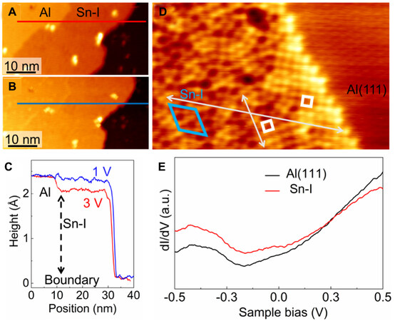
Figure 3. (A and B) STM images of a selected area with coexistence of Sn-I phase and bare substrate under different sample biases [3 V for (A) and 1 V for (B)]. (C) Height profiles along the corresponding lines in (A) (red curve) and (B) (blue curve). (D) The STM image of a boundary area between Sn-I phase and the bare substrate showing the square-like lattice at the boundary (-50 mV, 50 pA). (E) dI/dV spectra on Al(111) and Sn-I phase.
When the coverage of tin atoms is increased to 1 ML and above [Figure 4A], a second phase with stripe feature (Sn-II) appears on the surface covering the whole surface. With the atomic resolution STM image in Figure 4B, Sn-II phase is revealed to be square-like lattice with the lattice constant of 0.3 nm, which is the same as the atomic structure of the boundary between Sn-I phase and Al(111). Therefore, with the same lattice constant and lattice direction, Sn-II phase is thought to gradually form from Sn-I phase with increasing coverage at the boundary area. The difference is that Sn-II phase exhibits a 4 × 6 stripe structure
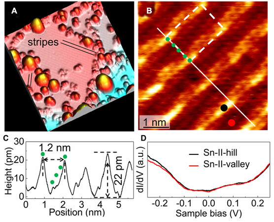
Figure 4. (A) STM image of the surface after deposition of > 1 ML Sn on Al(111) showing stripe structure (Sn-II phase) and abundant clusters on the surface (2.5 V, 50 pA, image size is 50 nm × 50 nm). (B) Atomic resolution STM image of Sn-II phase (16 mV, 900 pA). (C) Height profile along the white line in (B). (D) dI/dV spectra on the hill and valley of the stripe structure of Sn-II phase.
Here, the square-like tin allotrope, however, is rare in the epitaxial growth elemental films on hexagonal substrates which usually exhibit hexagonal or trigonal lattice geometries. The unusual difference in geometry between the epitaxial film and substrate can be explained by the decoupling effect of increased bonding strength between tin atoms at higher tin coverage. The formation of four-coordinate bonds in the square geometry can also decrease the number of unsaturated bonds and reduce the orbital hybridization with the substrate, thereby promoting the decoupling effect. This conjecture is supported by the fact that Sn nanoclusters appear on the surface of Sn-II as the coverage is much higher than 1 ML [Figure 4A], which indicates that Sn-II phase is acting as a “buffer” layer that decreases the interaction between the surplus tin atoms and the substrate and enables the formation of Sn nanocluster. The dI/dV spectra on Sn-II phase
CONCLUSIONS
In summary, two 2D tin allotropes with quasi-periodic lattice and square-like lattice are fabricated on Al(111) by epitaxial growth method at different tin coverages. Beyond sub-monolayer coverage, the enhanced decoupling effect occurs and induces a square-like lattice, which is rarely found among epitaxial elemental monolayers on metal substrates with hexagonal lattice. The presence of these two well-defined structures adds another degree of freedom to stanene and other 2D elemental monolayers beyond the honeycomb and buckled honeycomb lattices regarding the lattice symmetry design and tunning the interaction between epitaxial films and substrates.
DECLARATIONS
Authors’ contributionsMade substantial contributions to conception and design of the study and performed data analysis and interpretation: Feng H, Du Y
Performed data acquisition and provided administrative, technical, and material support: Feng H, Xu X, Liu Y, Zhuang J, Hao W, Dou SX
Availability of data and materialsNot applicable.
Financial support and sponsorshipThis work is supported by the National Natural Science Foundation of China (12074021, 12104033, 12004321, 12274016, 52073006), the Fundamental Research Funds for the Central Universities and Australian Research Council (LP180100722).
Conflicts of interestAll authors declared that there are no conflicts of interest.
Ethical approval and consent to participateNot applicable.
Consent for publicationNot applicable.
Copyright© The Author(s) 2023.
REFERENCES
1. Xu Y, Yan B, Zhang HJ, et al. Large-gap quantum spin hall insulators in tin films. Phys Rev Lett 2013;111:136804.
2. Zhu FF, Chen WJ, Xu Y, et al. Epitaxial growth of two-dimensional stanene. Nat Mater 2015;14:1020-5.
4. Deng J, Xia B, Ma X, et al. Epitaxial growth of ultraflat stanene with topological band inversion. Nat Mater 2018;17:1081-6.
5. Gou J, Kong L, Li H, et al. Strain-induced band engineering in monolayer stanene on Sb(111). Phys Rev Mater 2017;1:054004.
6. Liu Y, Gao N, Zhuang J, et al. Realization of strained stanene by interface engineering. J Phys Chem Lett 2019;10:1558-65.
7. Yuhara J, Fujii Y, Nishino K, et al. Large area planar stanene epitaxially grown on Ag(111). 2D Mater 2018;5:025002.
8. Xu C, Chan Y, Chen P, et al. Gapped electronic structure of epitaxial stanene on InSb(111). Phys Rev B 2018;97:035122.
9. Zang Y, Jiang T, Gong Y, et al. Realizing an epitaxial decorated stanene with an insulating bandgap. Adv Funct Mater 2018;28:1802723.
10. Maniraj M, Stadtmüller B, Jungkenn D, et al. A case study for the formation of stanene on a metal surface. Commun Phys 2019;2:2.
11. Zheng X, Zhang J, Tong B, Du R. Epitaxial growth and electronic properties of few-layer stanene on InSb(111). 2D Mater 2020;7:011001.
12. Zhao C, Li L, Zhang L, et al. Coexistence of robust edge states and superconductivity in few-layer stanene. Phys Rev Lett 2022;128:206802.
13. Tang P, Chen P, Cao W, et al. Stable two-dimensional dumbbell stanene: a quantum spin hall insulator. Phys Rev B 2014;90:121408.
14. Cao W, Tang P, Zhang S, Duan W, Rubio A. Stable dirac semimetal in the allotropes of group-IV elements. Phys Rev B 2016;93:241117.
15. Xu C, Wang Y, Han R, Tu H, Yan Y. Topological node line semimetal state in two-dimensional tetragonal allotrope of Ge and Sn. New J Phys 2019;21:033005.
16. Borlido P, Huran AW, Marques MAL, Botti S. Structural prediction of stabilized atomically thin tin layers. NPJ 2D Mater Appl 2019;3:1-5.
17. Niu T, Zhou W, Zhou D, et al. Modulating epitaxial atomic structure of antimonene through interface design. Adv Mater 2019;31:e1902606.
18. Zhou D, Meng Q, Si N, et al. Epitaxial growth of flat, metallic monolayer phosphorene on metal oxide. ACS Nano 2020;14:2385-94.
19. Nevalaita J, Koskinen P. Atlas for the properties of elemental two-dimensional metals. Phys Rev B 2018:97.
20. Zhang Z, Mannix AJ, Hu Z, et al. Substrate-induced nanoscale undulations of borophene on silver. Nano Lett 2016;16:6622-7.
21. Horcas I, Fernández R, Gómez-Rodríguez JM, Colchero J, Gómez-Herrero J, Baro AM. WSXM: a software for scanning probe microscopy and a tool for nanotechnology. Rev Sci Instrum 2007;78:013705.
Cite This Article
Export citation file: BibTeX | RIS
OAE Style
Feng H, Xu X, Liu Y, Zhuang J, Hao W, Du Y, Dou SX. Microstructural constructing 2D tin allotropes on Al(111): from quasi-periodic lattice to square-like lattice. Microstructures 2023;3:2023017. http://dx.doi.org/10.20517/microstructures.2023.01
AMA Style
Feng H, Xu X, Liu Y, Zhuang J, Hao W, Du Y, Dou SX. Microstructural constructing 2D tin allotropes on Al(111): from quasi-periodic lattice to square-like lattice. Microstructures. 2023; 3(3): 2023017. http://dx.doi.org/10.20517/microstructures.2023.01
Chicago/Turabian Style
Feng, Haifeng, Xun Xu, Yundan Liu, Jincheng Zhuang, Weichang Hao, Yi Du, Shi Xue Dou. 2023. "Microstructural constructing 2D tin allotropes on Al(111): from quasi-periodic lattice to square-like lattice" Microstructures. 3, no.3: 2023017. http://dx.doi.org/10.20517/microstructures.2023.01
ACS Style
Feng, H.; Xu X.; Liu Y.; Zhuang J.; Hao W.; Du Y.; Dou SX. Microstructural constructing 2D tin allotropes on Al(111): from quasi-periodic lattice to square-like lattice. Microstructures. 2023, 3, 2023017. http://dx.doi.org/10.20517/microstructures.2023.01
About This Article
Copyright

Data & Comments
Data
0

 Cite This Article 8 clicks

 Like This Article 31
likes
Like This Article 31
likes


Comments
Comments must be written in English. Spam, offensive content, impersonation, and private information will not be permitted. If any comment is reported and identified as inappropriate content by OAE staff, the comment will be removed without notice. If you have any queries or need any help, please contact us at support@oaepublish.com.