
Intrinsic supercurrent diode effect in NbSe2 nanobridge
 0
0Abstract
The significance of the superconducting diode effect (SDE) lies in its potential application as a fundamental component in the development of next-generation superconducting circuit technology. The stringent operating conditions at low temperatures have posed challenges for the conventional semiconductor diode, primarily due to its exceptionally high resistivity. In response to this limitation, various approaches have emerged to achieve the SDE, primarily involving the disruption of inversion symmetry in a two-dimensional superconductor through heterostructure fabrication. In this study, we present a direct observation of the supercurrent diode effect in a NbSe2 nanobridge with a length of approximately 15 nm, created using focused helium ion beam fabrication. Nonreciprocal supercurrents were identified, reaching a peak value of approximately 380 μA for each bias polarity at Bzmax = ± 0.2 mT. Notably, the nonreciprocal supercurrent can be toggled by altering the bias polarity. This discovery of the SDE introduces a novel avenue and mechanism through nanofabrication on a superconducting flake, offering fresh perspectives for the development of superconducting devices and potential circuits.
Keywords
INTRODUCTION
Nonreciprocal charge transport is a phenomenon commonly observed in semiconductors[1,2], characterized by an electron-hole asymmetric junction that produces an asymmetric current in response to positive and negative voltages. This behavior finds extensive applications in electronic devices, including diodes, a.c./d.c. converters, optical isolators, circulators, and microwave diodes across a wide frequency spectrum[3-5]. Among these, the p-n junction, a well-established device in logic and computation, is structured by the hetero-interface of a p-type and an n-type semiconductor, resulting in an asymmetric current-voltage characteristic (IVC). However, the applicability of semiconductor junctions in quantum circuits is limited by the requirement to operate at extremely low temperatures to avoid thermal excitation. To address this challenge, a practical solution is found in the nonreciprocal supercurrent, known as the superconducting diode effect (SDE)[6]. The SDE exhibits nonreciprocity in non-dissipative superconducting current, allowing it to flow exclusively in one direction. Serving as the superconducting counterpart to a semiconducting diode, this effect has the potential to emerge as a novel non-dissipative circuit element, akin to traditional diodes. This characteristic opens up exciting possibilities in the realms of superconducting electronics[7], superconducting spintronics[8,9], and quantum information and communication technology[10,11].
In recent years, various methods have been proposed to realize the SDE. The initial discovery of SDE was reported by Ando et al., who investigated a junction-free superconducting [Nb/V/Ta]n superlattice, breaking both spatial-inversion and time-reversal symmetries[12]. Subsequent research by the same team introduced another implementation of zero-field SDE using noncentrosymmetric [Nb/V/Co/V/Ta] superconducting films with 20 multilayers, demonstrating the achievability of field-free SDE through noncentrosymmetric superconductor/ferromagnet multilayers[13]. A notable advancement stems from the study of a NbSe2/Nb3Br8/NbSe2 Josephson junction, functioning as a field-free SDE due to the asymmetric Josephson tunneling induced by rotational symmetry breaking from Nb3Br8 on NbSe2/Nb3Br8 interfaces[14]. Moreover, a supercurrent diode effect was observed in few-layer NbSe2 sandwiched between BN. This observation results from the breaking of inversion symmetry caused by the presence of a few layers of
This study presents the observation of intrinsic SDE in a NbSe2 nanobridge, created using a focused helium ion microscope. Nonreciprocal critical currents are evident without the need for artificially breaking inversion symmetry when a nonzero magnetic field is applied. Current-voltage (I-V) mapping illustrates the asymmetry of the critical current (Ic) concerning the magnetic field under bias polarities at Bz= ± 0.2 mT. A demonstrated example of a bias-polarity-controlled superconductivity diode is provided.
MATERIALS AND METHODS
Thin NbSe2 flakes are mechanically exfoliated onto a polydimethylsiloxane (PDMS) film positioned on a glass slide. Subsequently, the PDMS is stamped onto the pre-prepared electrode using a micromanipulator located beneath a microscope. The sample transfer process is conducted within a glove box filled with argon gas.
The microbridge sample was fabricated using a Laser Direct-Write Lithography System (Durham Magneto Optics Ltd) and a reactive ion beam etching system (Advance Vacuum Scandinavia AB). Figure 1A illustrates the schematic representation of the typical device. The chosen NbSe2 crystal for this study has a thickness of approximately 15.4 nm [Supplementary Figure 1]. Electrical contacts and microbridge strips
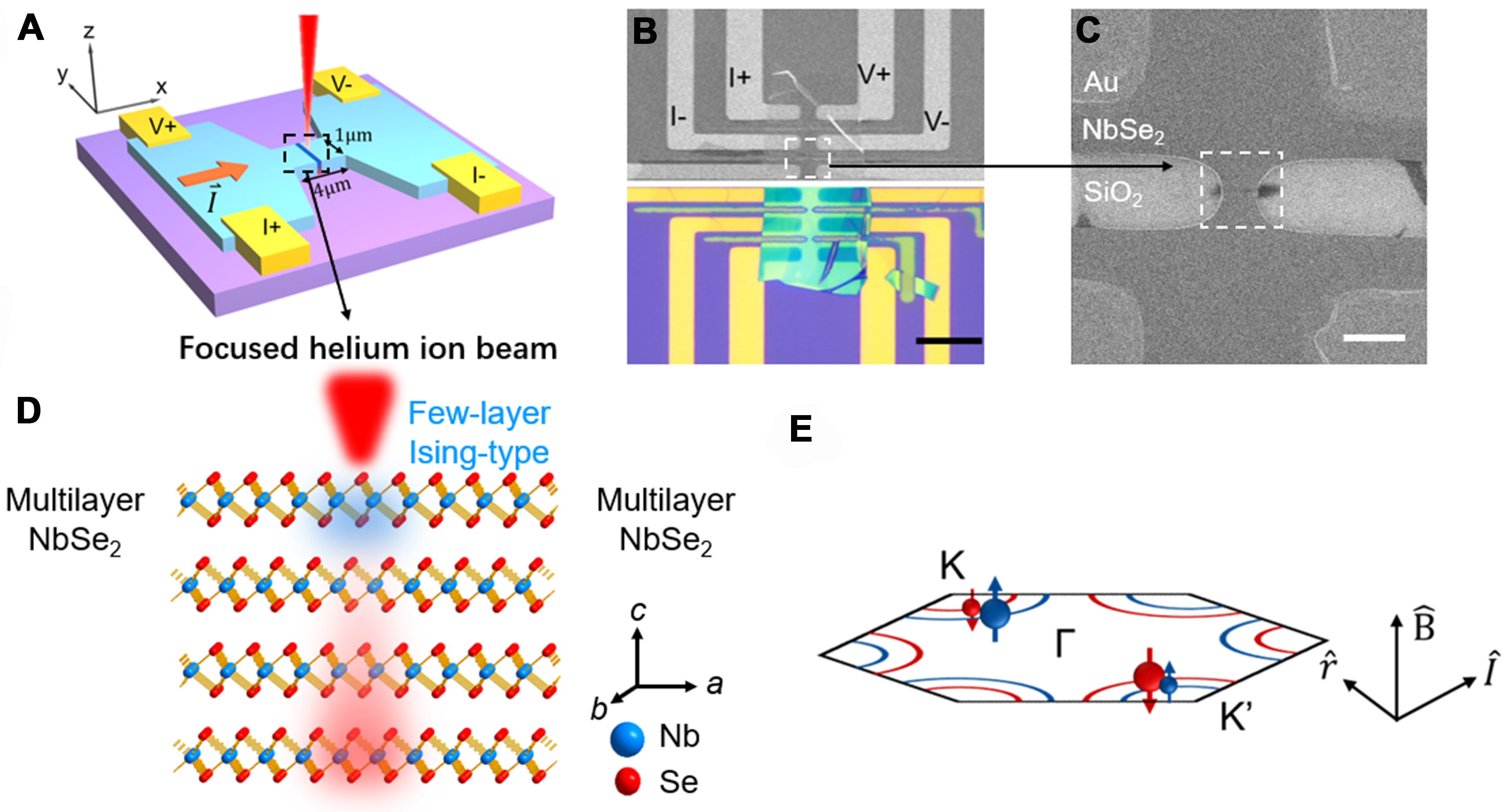
Figure 1. (A) Schematic illustration of the measurement configuration. The orange arrow indicates the supercurrent pathway, and the red laser indicates the focused helium ion beam creating a weakly coupled junction in the multilayer NbSe2. The central constriction is about 1 μm wide and 15 nm long. The direction of the supercurrent is defined along the x-axis, while the z-axis is perpendicular to the crystal plane; (B) Artistic representation of the focused helium ion beam etching the multilayer NbSe2. The crystal structure is that of NbSe2; (C) SEM (upper) and optical (lower) image of the device. The nanobridge is made by ion beam etching, and an Ohmic contact is made by the pick-up and transfer method; scale bar, 20 μm; (D) A zoom-in image of the dashed rectangular area shown in (B). The color change reflects the change in electrical conductivity, which can be observed; (E) Illustration depicting type-I Ising superconductivity: the pairing of electrons in valleys with opposite spin splitting.
The as-patterned nanobridge measures approximately 15 nm in length and 1 μm in width, depicted as a red and blue gradient area in Figure 1A. The red area signifies the region where superconductivity is disrupted, while the blue area represents NbSe2 reaching the 2D limit. A schematic diagram of the helium-ion-beam milling process of NbSe2 is presented in Figure 1B. During the process, He+ implantation into the NbSe2 crystal can lead to preferential sputtering of selenium atoms within the 2D transition-metal dichalcogenides (TMDs)[20], resulting in the degradation of superconductivity in the irradiated region (red area). Notably, vacancy defects caused by recoil ions serve as the primary source of superconductivity disruption. Consequently, the surface, in contrast to the underlying NbSe2, can be considered nearly undamaged. As the radiation linear fluence increases, the influence depth of He ions extends, subsequently reducing the thickness of the superconducting NbSe2. This process may facilitate the formation of Ising pairing in few-layer NbSe2 (blue area).
Electrical transport measurements were conducted utilizing a Physical Property Measurement System (PPMS-Dynacool, Quantum Design) with the external electric meter comprising a Keithley 2400 as the current source and a Keithley 2182 as the voltage meter. The investigation of transport properties employed conventional four-terminal methods.
RESULTS AND DISCUSSION
In monolayer or few-layer NbSe2, the in-plane inversion symmetry is disrupted. Consequently, the concurrent impact of the Zeeman effect and substantial intrinsic spin-orbit interactions gives rise to an electron-spin-locking phenomenon along the out-of-plane direction[19,21-23] [Figure 1E]. Ising-type superconducting pairing symmetry emerges in NbSe2 due to the reverse spin splitting within the valence bands near valleys K and K’. This phenomenon gives rise to intervalley spin-momentum-locked spin-singlet Cooper pairing between two electrons, characterized by opposing momenta and antiparallel out-of-plane spins.
The directions of the inversion symmetry break
Figure 2 illustrates the nonreciprocal transport properties of the NbSe2 nanobridge under varying irradiation linear fluences. Figure 2A-C depicts three pairs of IVCs corresponding to the magnetic fields applied along the
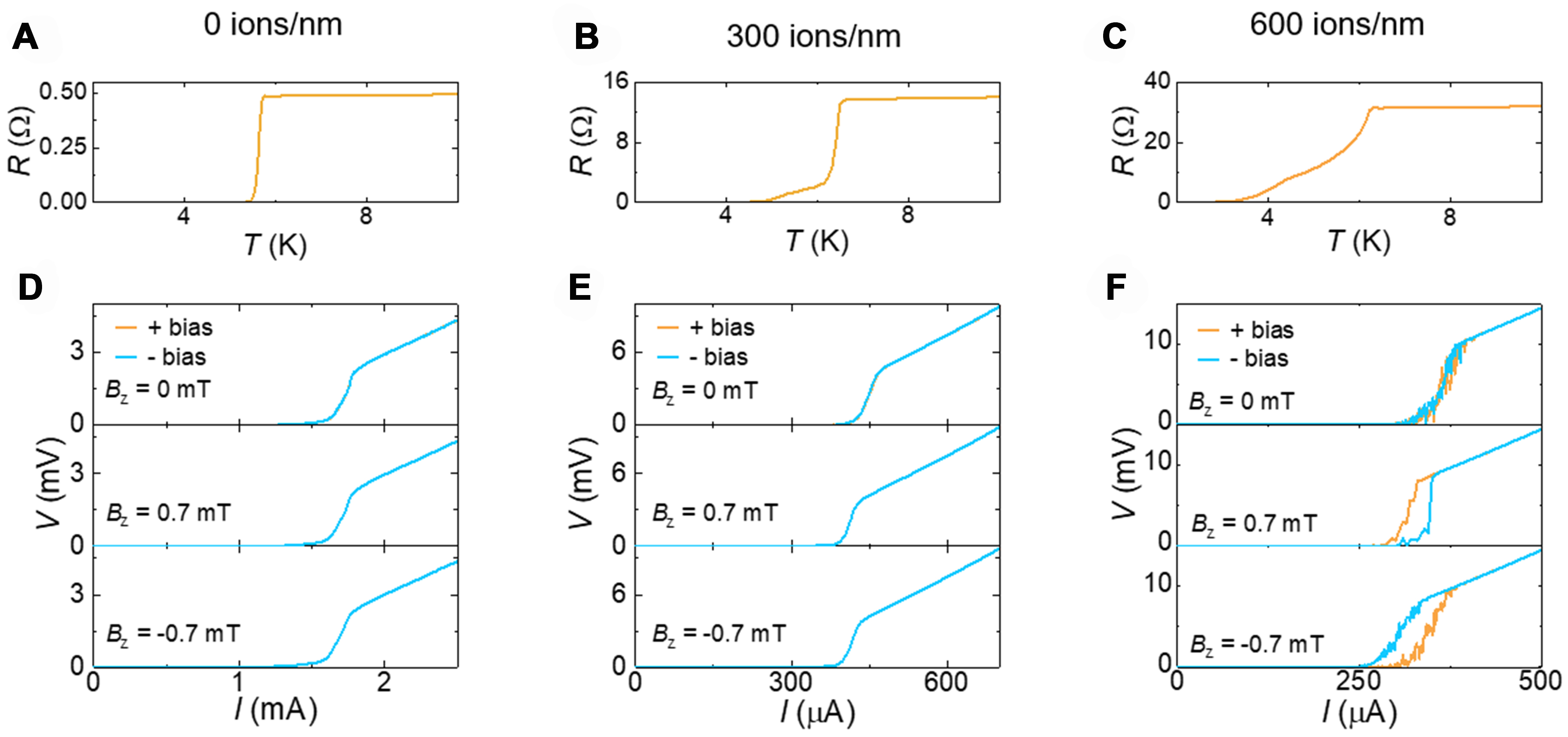
Figure 2. (A-C) Current-voltage characteristics were measured at 2 K, considering opposite bias polarities (current directions) in a
As the irradiation linear fluence increases to 600 ions/nm, a robust SDE becomes evident, as depicted in the I-V curves in Figure 2C. Notably, a significant disparity exists in linear fluences between Ic+ and |Ic-| in the critical current for the two supercurrent orientations. The sign of Δ = Ic+ - |Ic-| changes with the reversal of the magnetic field Bz, confirming that Δ is intrinsically determined by the magnetic field. The I-V loop further excludes the influence of thermal effects [Supplementary Figure 2]. It is essential to note that the nanobridge appears to be slightly damaged under helium ion irradiation, as evidenced by optical microscope and SEM images [Figure 1C and D]. A zoom-in image can clearly show the area of helium ion radiation framed by a dashed rectangle. We hypothesize that helium ions might influence chemical bonds or even induce doping[25,26], rather than causing a direct etching effect. Similar to the outcomes of electron beam irradiation[27], helium ion irradiation can introduce disorders into thin crystals, potentially suppressing superconductivity. Temperature dependence of resistance [Figure 2D-F] exhibits a broadened superconducting transition region with increasing linear fluences, which indicates the degradation of superconductivity in the nanobridge. Consequently, our focus shifts to the study of the sample under
The I-V values at 2 K under various magnetic fields are presented in Figure 3A, where the color bar reflects the differential resistance (dV/dI). An enlarged view around zero field is provided in Figure 3B, revealing a distinct asymmetric behavior. The maximum of the differential resistance is defined as the critical current

Figure 3. (A) A color map of critical current in the plane of magnetic field at 2 K, and a color bar shows the value of dV/dI. An apparent current asymmetry with respect to the magnetic field can be observed. The critical current can be extracted, as shown in (C); (B) A magnification of (A). The red dotted line marks the zero-field position; (C) Nonreciprocal critical current (Ic) as a function of Bz, with positive bias (orange) and negative bias (red), exhibiting symmetry across reflection about Bz = 0. The critical current peaks at a nonzero |Bzmax| = 0.2 mT, indicated by labeled orange and blue arrows.
The substantial rise in the critical current is vital as it dismisses the possibility of the nonreciprocal supercurrent originating from Joule heating[15]. Although the origin of the supercurrent diode effect in NbSe2 requires further investigation, several potential explanations can be considered. These include the interplay between Meissner currents and barriers for vortex entry[28,29], vortex flow in asymmetric pinning potentials[19], and the influence of valley-Zeeman spin-orbit interaction[15]. It is noteworthy that the observed behavior closely resembles the characteristics of NbSe2 in the 2D limit[19,21,22,30,31], despite our sample having a thickness of approximately 15.4 nm. However, upon dimension reduction in the nanobridge, phenomena akin to those observed in Josephson junctions emerge [Supplementary Figure 4]. It is noteworthy that in non-uniform Josephson junctions, the dominance of Josephson vortex motion leads to an asymmetric Fraunhofer pattern[32,33]. A recent experimental study has successfully achieved SDE by introducing a non-uniform current and a single Abrikosov vortice in the junction electrodes[34]. Actually, the non-uniform penetration of helium ions can induce a non-uniform supercurrent, even when the current is uniform based on the geometry of the device [Supplementary Figure 6]. This inhomogeneity can amplify the SDE, particularly in the presence of a large critical current density, 26.7 mA·μm-2 in this instance.
The primary outcome of our observations indicates that the supercurrent diode effect in the NbSe2 nanobridge is governed by the out-of-plane magnetic field. Based on this idea, we demonstrated bias-polarity-controlled SDE at 2 K, 0.2 mT, where the |Ic-| reaches the maximum [Figure 4]. The values of Ic+ and |Ic-| are 345 and 380 μA, respectively. A square-wave excitation with an amplitude of 340 μA is applied
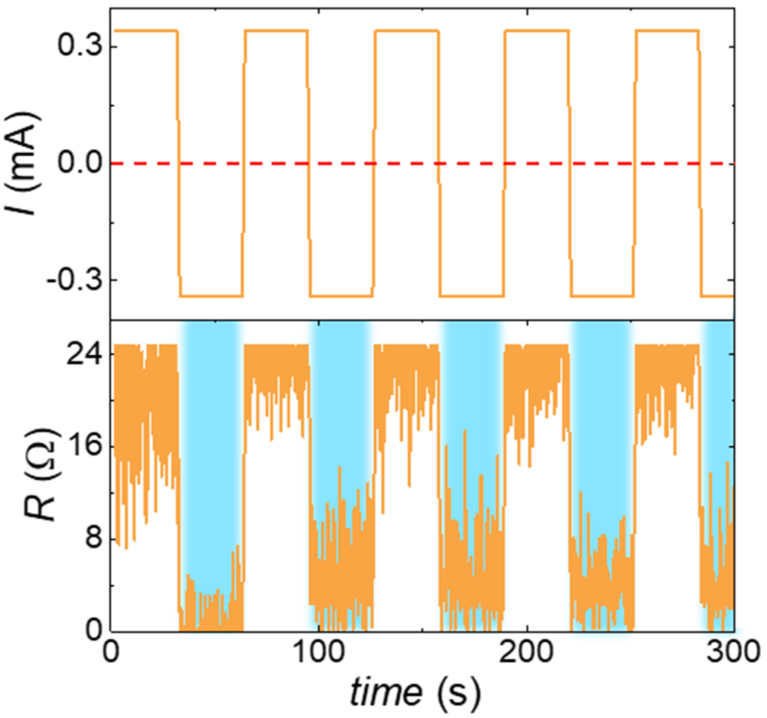
Figure 4. Controllable superconducting diode. The top panel displays the square-wave excitation applied at 2 K with an amplitude of 340 μA (between Ic+ and |Ic-|) under a magnetic field of 0.2 mT. The coincidentally measured junction voltage is presented in the bottom panel. In this depiction, the blue shaded region represents the superconducting state, where the voltage remains zero under negative current bias. Conversely, the white region signifies the normal state, with a high voltage observed during positive current bias. The red dotted line denotes the zero line.
CONCLUSIONS
In conclusion, we have illustrated a supercurrent diode effect in a NbSe2 nanobridge fabricated using a focused helium ion microscope. Our findings indicate that this effect is governed by the out-of-plane magnetic field, presenting a deviation from observations in Rashba superconductors. Nonreciprocal critical currents can be well turned under bias polarities at Bzmax = ± 0.2 mT. Helium ions break the superconductivity at a certain depth and shrink the thickness of the superconductor to 2D limit. The findings suggest that the supercurrent diode effect may be linked to the inversion symmetry breaking caused by Ising SOC in a few layers of NbSe2 and can be improved by heterogeneous penetration of helium ions. This insight offers a potential avenue for comprehending and optimizing the performance of the supercurrent diode effect, with implications for its application in superconducting logic and memory devices.
DECLARATIONS
Acknowledgments
Thanks to the technical support from the Soft Matter Nanofab (SMN180827) and Center for High-resolution Electron Microscopy (CħEM), SPST, ShanghaiTech University (EM02161943).
Authors’ contributions
Made substantial contributions to the conception and design of the study and performed data analysis and interpretation: Zhang Y
Transmission electron microscopy (TEM) and ion damage calculation: Cai J, Cao K
Writing, review and editing: Zhang Y, Wu Y, Li J
Investigation: Dong P, He J, Ding Y, Wang J, Zhou X
Availability of data and materials
Not applicable.
Financial support and sponsorship
This research was supported in part by the Ministry of Science and Technology (MOST) of China (No. 2022YFA1603903), the National Natural Science Foundation of China (Grant No. 12004251, No. 12104302, and No. 12104303), the Science and Technology Commission of Shanghai Municipality, the Shanghai Sailing Program (Grant No. 21YF1429200), and the start-up funding from ShanghaiTech University, Beijing National Laboratory for Condensed Matter Physics, the Interdisciplinary Program of Wuhan National High Magnetic Field Center (WHMFC202124), the Science and Technology Commission of the Shanghai Municipality (21JC1405100).
Conflicts of interest
All authors declared that there are no conflicts of interest.
Ethical approval and consent to participate
Not applicable.
Consent for publication
Not applicable.
Copyright
© The Author(s) 2024.
Supplementary Materials
REFERENCES
1. Scaff JH, Ohl RS. Development of silicon crystal rectifiers for microwave radar receivers. Bell Syst Tech J 1947;26:1-30.
2. Shockley W. The theory of p-n junctions in semiconductors and p-n junction transistors. Bell Syst Tech J 1949;28:435-89.
3. Tokura Y, Nagaosa N. Nonreciprocal responses from non-centrosymmetric quantum materials. Nat Commun 2018;9:3740.
4. Saito M, Ishikawa K, Taniguchi K, Arima T. Magnetic control of crystal chirality and the existence of a large magneto-optical dichroism effect in CuB2O4. Phys Rev Lett 2008;101:117402.
5. Okamura Y, Kagawa F, Mochizuki M, et al. Microwave magnetoelectric effect via skyrmion resonance modes in a helimagnetic multiferroic. Nat Commun 2013;4:2391.
7. Braginski AI. Superconductor electronics: status and outlook. J Supercond Nov Magn 2019;32:23-44.
9. Cai R, Žutić I, Han W. Superconductor/ferromagnet heterostructures: a platform for superconducting spintronics and quantum computation. Adv Quantum Tech 2023;6:2200080.
10. Wendin G. Quantum information processing with superconducting circuits: a review. Rep Prog Phys 2017;80:106001.
12. Ando F, Miyasaka Y, Li T, et al. Observation of superconducting diode effect. Nature 2020;584:373-6.
13. Narita H, Ishizuka J, Kawarazaki R, et al. Field-free superconducting diode effect in noncentrosymmetric superconductor/ferromagnet multilayers. Nat Nanotechnol 2022;17:823-8.
14. Wu H, Wang Y, Xu Y, et al. The field-free Josephson diode in a van der Waals heterostructure. Nature 2022;604:653-6.
15. Bauriedl L, Bäuml C, Fuchs L, et al. Supercurrent diode effect and magnetochiral anisotropy in few-layer NbSe2. Nat Commun 2022;13:4266.
16. de Vries FK, Portolés E, Zheng G, et al. Gate-defined Josephson junctions in magic-angle twisted bilayer graphene. Nat Nanotechnol 2021;16:760-3.
17. Jeon KR, Kim JK, Yoon J, et al. Zero-field polarity-reversible Josephson supercurrent diodes enabled by a proximity-magnetized Pt barrier. Nat Mater 2022;21:1008-13.
18. Anwar MS, Nakamura T, Ishiguro R, et al. Spontaneous superconducting diode effect in non-magnetic Nb/Ru/Sr2RuO4 topological junctions. Commun Phys 2023;6:290.
19. Zhang E, Xu X, Zou YC, et al. Nonreciprocal superconducting NbSe2 antenna. Nat Commun 2020;11:5634.
20. Stanford MG, Pudasaini PR, Belianinov A, et al. Focused helium-ion beam irradiation effects on electrical transport properties of few-layer WSe2: enabling nanoscale direct write homo-junctions. Sci Rep 2016;6:27276.
21. Xi X, Wang Z, Zhao W, et al. Ising pairing in superconducting NbSe2 atomic layers. Nature Phys 2016;12:139-43.
22. de la Barrera SC, Sinko MR, Gopalan DP, et al. Tuning Ising superconductivity with layer and spin-orbit coupling in two-dimensional transition-metal dichalcogenides. Nat Commun 2018;9:1427.
23. Yi H, Hu LH, Wang Y, et al. Crossover from Ising- to Rashba-type superconductivity in epitaxial Bi2Se3/monolayer NbSe2 heterostructures. Nat Mater 2022;21:1366-72.
24. Edelstein VM. The Ginzburg - Landau equation for superconductors of polar symmetry. J Phys Condens Matter 1996;8:339.
25. Matsui H, Nishijima G, Matsumoto A, Yamaguchi I, Manabe T, Sohma M. Nonreciprocal critical current in an obliquely ion-irradiated YBa2Cu3O7 film. Appl Phys Lett 2023;122:172601.
26. Palau A, Monton C, Rouco V, Obradors X, Puig T. Guided vortex motion in YBa2Cu3O7 thin films with collective ratchet pinning potentials. Phys Rev B 2012;85:012502.
27. Cho K, Kończykowski M, Teknowijoyo S, et al. Using controlled disorder to probe the interplay between charge order and superconductivity in NbSe2. Nat Commun 2018;9:2796.
28. Hou Y, Nichele F, Chi H, et al. Ubiquitous superconducting diode effect in superconductor thin films. Phys Rev Lett 2023;131:027001.
29. Gutfreund A, Matsuki H, Plastovets V, et al. Direct observation of a superconducting vortex diode. Nat Commun 2023;14:1630.
30. Sohn E, Xi X, He WY, et al. An unusual continuous paramagnetic-limited superconducting phase transition in 2D NbSe2. Nat Mater 2018;17:504-8.
31. Falson J, Xu Y, Liao M, et al. Type-II Ising pairing in few-layer stanene. Science 2020;367:1454-7.
32. Goldman AM, Kreisman PJ. Meissner effect and vortex penetration in Josephson junctions. Phys Rev 1967;164:544-7.
33. Krasnov VM, Oboznov VA, Pedersen NF. Fluxon dynamics in long Josephson junctions in the presence of a temperature gradient or spatial nonuniformity. Phys Rev B 1997;55:14486-98.
Cite This Article
Export citation file: BibTeX | RIS
OAE Style
Zhang Y, Cai J, Dong P, He J, Ding Y, Wang J, Zhou X, Cao K, Wu Y, Li J. Intrinsic supercurrent diode effect in NbSe2 nanobridge. Microstructures 2024;4:2024018. http://dx.doi.org/10.20517/microstructures.2023.73
AMA Style
Zhang Y, Cai J, Dong P, He J, Ding Y, Wang J, Zhou X, Cao K, Wu Y, Li J. Intrinsic supercurrent diode effect in NbSe2 nanobridge. Microstructures. 2024; 4(2): 2024018. http://dx.doi.org/10.20517/microstructures.2023.73
Chicago/Turabian Style
Zhang, Yiwen, Jiliang Cai, Peng Dong, Jiadian He, Yifan Ding, Jinghui Wang, Xiang Zhou, Kecheng Cao, Yueshen Wu, Jun Li. 2024. "Intrinsic supercurrent diode effect in NbSe2 nanobridge" Microstructures. 4, no.2: 2024018. http://dx.doi.org/10.20517/microstructures.2023.73
ACS Style
Zhang, Y.; Cai J.; Dong P.; He J.; Ding Y.; Wang J.; Zhou X.; Cao K.; Wu Y.; Li J. Intrinsic supercurrent diode effect in NbSe2 nanobridge. Microstructures. 2024, 4, 2024018. http://dx.doi.org/10.20517/microstructures.2023.73
About This Article
Special Issue
Copyright

Data & Comments
Data
0

 Cite This Article 1 clicks

 Like This Article 1
likes
Like This Article 1
likes


Comments
Comments must be written in English. Spam, offensive content, impersonation, and private information will not be permitted. If any comment is reported and identified as inappropriate content by OAE staff, the comment will be removed without notice. If you have any queries or need any help, please contact us at support@oaepublish.com.