
Microstructural evolution and ferroelectricity in HfO2 films


Abstract
Ferroelectric (FE) materials, which typically adopt the perovskite structure with non-centrosymmetry and exhibit spontaneous polarization, are promising for applications in memory, electromechanical and energy storage devices. However, these advanced applications suffer from the intrinsic limitations of perovskite FEs, including poor complementary metal oxide semiconductor (CMOS) compatibility and environmental issues associated with lead. Hafnium oxide (HfO2), with stable bulk centrosymmetric phases, possesses robust ferroelectricity in nanoscale thin films due to the formation of non-centrosymmetric phases. Owing to its high CMOS compatibility and high scalability, HfO2 has attracted significant attention. In the last decade, significant efforts have been made to explore the origin of the ferroelectricity and factors that influence the FE properties in HfO2 films, particularly regarding the role of microstructure, which is vital in clarifying these issues. Although several comprehensive reviews of HfO2 films have been published, there is currently no review focused on the relationship between microstructure and FE properties. This review focuses on the microstructure-property relationships in FE polycrystalline and epitaxial HfO2 films. The crystallographic structures and characterization methods for HfO2 polymorphs are first discussed. For polycrystalline HfO2 films, the microstructure-FE properties relationships, driving force and kinetic pathway of phase transformations under growth parameters or external stimuli are reviewed. For epitaxial films, the lattice matching relations between HfO2 films and substrates and the corresponding impact on the FE properties are discussed. The FE properties between polycrystalline and epitaxial HfO2 films are compared based on their different microstructural characteristics. Finally, a future perspective is given for further investigating FE HfO2 films.
Keywords
INTRODUCTION
Ferroelectric (FE) materials have non-centrosymmetric structures and present spontaneous electrical polarity that can be reversed by an applied electric field, which makes them promising for electromechanical, memory and energy storage devices[1]. Conventional perovskite FE devices can be fabricated from lead-based Pb(Zr,Ti)O3[2-4], lead-free BaTiO3[5,6] and relaxor-based (PbMg1/3Nb2/3O3)1-x-(PbTiO3)x[7-9] materials. However, these FE devices suffer from various problems during the device manufacturing process and usage, including a requirement for large thicknesses (~100 nm)[10], integration difficulties with modern complementary metal oxide semiconductor (CMOS) technology[11], small bandgaps (3-4 eV)[12,13] and environmental issues due to toxic elements like Pb and Ba[14]. Therefore, the development of lead-free FE materials that overcome these barriers is emerging.
HfO2 films are CMOS compatible and have been extensively used for high K metal-gate technology[15]. After ferroelectricity in HfO2 thin films was reported in 2011[16], HfO2 films have attracted significant interest as next-generation FEs due to their excellent properties[17-35]. First, HfO2 films are CMOS compatible due to their small thickness (~10 nm) and high resistance to hydrogen and the etching process, which makes HfO2 films promising for one transistor and one transistor-one capacitor FE memories, as well as nanoscale FE devices[36]. Second, the simple chemistry of HfO2 also makes it less prone to the perturbing effects that occur in multicomponent materials during deposition processes and simplifies theoretical studies, including ab-initio simulations[37-41]. In addition, they have a large bandgap (> 5 eV) and strong bonds between O and Hf, which can mitigate the leakage current and reliability problems commonly observed in perovskite FEs[42]. Thus, these listed advantages, together with environmental-friendly components, make them promising for commercial FE memory devices.
After almost a decade of development, materials synthesis methods and property/structural characterization techniques have been well developed for polycrystalline HfO2 films[18,21,22,25,43,44]. Excellent FE performance (e.g., remanent polarization[45-47] up to 40 μC·cm-2, coercive field[19] of ~1-2 MV cm-1, endurance of ~1011 cycles[48] and switching time[49] of ~360 ps) has been reported in HfO2 films with thicknesses of less than
Although there have been significant developments in the fundamental understanding and device performance of polycrystalline FE HfO2 films, several limitations remain. First, compared to their perovskite counterparts, HfO2 films possess robust ferroelectricity when the sample thickness is smaller than 100 nm, which is quite unusual. The microscopic mechanism that stabilizes the FE phase by the factors mentioned above is still not well understood, despite many macroscopic experiments having been carried out[32,33,37,38,57,58]. While transmission electron microscopy (TEM) is a powerful tool for explorations of the microscopic mechanisms in FEs[59-61], the characterization of polycrystalline HfO2 films with nanometer grain sizes is not an easy task because of the frequent grain overlapping along the electron beam direction and the random crystalline orientations. Second, the ferroelectricity of HfO2 films suffers from their polycrystalline characteristics, particularly the existence of non-FE phases and grain boundaries[62]. The coexistence of FE and non-FE phases contributes to statistical non-uniformity in FE properties and device instability, where the remnant polarization (Pr) increases with electric cycling (the “wake-up” process). These two issues are significant for devices[33]. Furthermore, the accumulation of oxygen vacancies at grain boundaries leads to subsequent permanent conduction paths, resulting in device fatigue[25]. Therefore, both fundamental investigations and practical applications have illustrated the need for systematic studies of high-quality epitaxial HfO2 thin films in terms of microstructural characterization and microstructure-FE property relations to accurately regulate the FE properties in HfO2 films.
In 2015, Shimizu et al.[63] reported epitaxial orthorhombic YO1.5-substituted HfO2 (Y:HfO2) thin films grown by pulsed laser deposition (PLD). Ferroelectricity was observed in epitaxial 7%-Y:HfO2 films deposited on (110) yttrium oxide-stabilized zirconium oxide (YSZ) single crystalline substrates using Sn-doped In2O3 (ITO) as the bottom electrode[63,64]. Since then, other groups have also reported epitaxial FE HfO2-based films on other substrates, including Si and SrTiO3[29,65,66]. Lattice matching strain is the dominant factor in stabilizing the FE phases in epitaxial HfO2 films[67,68]. A single FE phase exists in epitaxial HfO2 thin films instead of the coexistence of FE and non-FE phases in their polycrystalline counterparts. A high polarization of up to
The macroscopic performance of FE materials is dominated by their microstructures[71-73], which can be altered by dopants[20,74,75], film thickness[50,76-78], thermal expansion and epitaxial strain[67,68,79,80]. In addition, mechanical, electrical, electromechanical and thermoelectric properties are crucial factors for the device applications of FE HfO2 materials. These properties are sensitive to changes in the embedded microstructures. Therefore, the observation of the corresponding microstructural evolution under various growth parameters and external stimuli is necessary for understanding their structure-property relations[22,23].
There have been several review articles of FE HfO2 films that have focused on film deposition, macroscopic FE properties, device fabrication and defect chemistry[36,51,62,75,81-89]. However, none of them deal with the relationship between microstructure and macroscopic FE properties, despite the fact that there has been a large number of publications that consider the microstructures of HfO2 FEs since the first demonstration of ferroelectricity in HfO2 films[16,18]. Therefore, a review focusing on the microstructure-FE behavior in HfO2 films is urgently required. Since the existing phases in polycrystalline and epitaxial films are quite different, we place particular emphasis on these films. For example, considering the coexistence of FE and non-FE polymorphs in polycrystalline HfO2 films, the FE phase fraction adjusted by growth parameters and microstructural evolutions under external stimuli are emphasized. Single-crystal HfO2 films can be obtained by size effect and epitaxial strain between the films and electrodes/substrates, thus the different matching relations between HfO2 films and substrates are focused on, in which the microstructure of the interfacial region between HfO2 films and electrodes/substrates is given particular attention.
In this review, we first introduce the polymorphs of HfO2, the characterization techniques for microstructures and the identification methods of FE phases. For polycrystalline HfO2 films, we review their growth methods, the impacts of growth parameters on the FE phase fraction and properties, and the phase transformations under external stimuli, e.g., temperature and electric loading. The thermodynamic driving force and kinetic pathway for phase transformation, which are vital for adjusting the FE phase fraction for the FE properties, are also discussed in this context. In epitaxial HfO2 films, microstructures and FE properties are controlled by lattice mismatch and interfacial chemistry between HfO2 films and electrodes/substrates, which are also reviewed here. The microstructures and FE behaviors (polarization, wake-up stage and device fatigue) in polycrystalline and epitaxial HfO2 films are then compared. Finally, the major conclusions are given and outstanding issues for future investigation in the field are presented.
IDENTIFICATION OF FE PHASES IN HfO2 FILMS
It once seemed impossible to observe ferroelectricity in nanoscale HfO2 films for two reasons: (1) a non-centrosymmetric crystal structure is necessary for FEs, but previously reported polymorphs of HfO2 are centrosymmetric, and (2) according to our knowledge of conventional perovskite FEs, it is unlikely to have nanoscale FEs. Therefore, it is important to identify FE phases in HfO2.
Polymorphs of bulk HfO2
Bulk HfO2 crystals present different polymorphs depending on the temperature and pressure. The left branch of Figure 1 lists the stable crystal structures reported in bulk HfO2 in the sequence based on symmetry reduction from the highest-symmetry cubic phase (C-phase, space group Fm$$\bar 3$$m) that exists above 2773 K[38]. During the cooling process, the C-phase transforms to a tetragonal phase (T-phase, space group P42/nmc) at 2773 K by symmetry reduction and then to a monoclinic phase (M-phase, space group P21/c) at 1973 K[90]. The M-phase is the most stable phase at room temperature and atmospheric pressure. At high pressure, bulk HfO2 has two orthorhombic polymorphs, denoted as orthoI (space group Pcba) and orthoII (space group Pmna)[91]. OrthoI is transformed from the T-phase by symmetry reduction under pressures between 4 and 14.5 GPa. OrthoI changes to orthoII with a pressure above 14.5 GPa and the transition pressure is almost independent of temperature[92]. All of these polymorphs have a center of symmetry, which is marked by the green point in each structure in the left branch of Figure 1. The centrosymmetric feature of these structures cannot induce ferroelectricity.
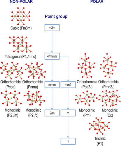
Figure 1. Symmetry-reduction flowchart of low energy phases of HfO2, starting from the C-phase. The left branch shows stable non-polar phases and the right branch presents polar phases obtained from first-principles calculations. Dark yellow and red spheres represent hafnium and oxygen atoms, respectively, while green spheres indicate the center of symmetry of the centrosymmetric phases[38].
Identification of FE HfO2 phases
Although the stable bulk HfO2 phases are centrosymmetric, HfO2 films with a nanoscale thickness, as well as properly doped HfO2 bulk crystals, can show another landscape. Compared with undoped bulk HfO2 crystals, atomic layer deposition (ALD) processed undoped HfO2 films with a thickness of 6 nm have robust ferroelectricity due to the formation of the FE O-phase under a nanoscale grain size effect[93]. These FE properties can be further enhanced by lowering the oxidant dose[94] and modulating the water pulse time[95] during the ALD process. In addition, ferroelectricity can also be stabilized in bulk HfO2 single crystals after 12% yttrium doping and a fast quenching process[34]. However, the most common and robust ferroelectricity is observed in nano HfO2 films doped with various elements.
The first report confirming robust ferroelectricity in HfO2-based materials was for Si-doped HfO2 (Si:HfO2) films with a thickness of 10 nm, in which the formation of a non-centrosymmetric O-phase (space group Pbc21) analogous to Mg:ZrO2 was also observed by grazing incidence X-ray diffraction measurements[16]. To identify the accurate atomic occupation of this FE structure in HfO2, density functional theory (DFT) calculations were firstly used to predict polar O-phases. First-principles calculations suggested that the two most viable FE phases are Pca21 and Pmn21 and that these two non-centrosymmetric equilibrium phases have similar free energies[38]. As shown in the right branch of Figure 1, the non-centrosymmetric structures with space groups of Pca21 and Pmn21can be obtained by distorting the P42/nmc structure along the [110] and [100] directions, respectively. The lattice parameters of these phases are summarized in
Lattice parameters of HfO2 polymorphs
| Polymorphs | a (Å) | b (Å) | c (Å) | β (°) | Notes | Source |
| M (P21/c) | 5.120 | 5.180 | 5.300 | 99°11' | XRD, 1970[96] | |
| T (P42/nmc) | 5.140 | 5.250 | 90° | 1920 °C | XRD, 1954[90] | |
| 5.1750 | 5.325 | 2000 °C | XRD, 1975[97] | |||
| NP-O (Pbcm) | 5.054 | 5.270 | 5.115 | 2.6 GPa | XRD[98] | |
| NP-O (Pbca) | 5.230 | 10.020 | 5.060 | XRD | ||
| P-O (Pmn21) | 3.415 | 5.182 | 3.834 | DFT, 2014[38] | ||
| P-O (Pca21) | 5.290 | 5.010 | 5.080 | DFT | ||
| 5.230 | 5.000 | 5.050 | Gd:HfO2 | XRD, 2015[53] | ||
| 5.240 | 5.060 | 5.070 | Gd:HfO2 | STEM, 2015[32] | ||
| 5.240 | 5.010 | 5.050 | Hf1/2Zr1/2O2 | XRD, 2012[74] | ||
| P-R (R3) | 7.106 | 7.106 | 9.016 | γ = 120° | Bulk HfO2 | First-principles calculation, 2018[29] |
| P-R (R3m) | 7.134 | 7.134 | 8.741 | Bulk HfO2 | ||
| 6.683 | 6.683 | 10.041 | compressed | |||
Sang et al.[32] confirmed the Pca21 phase in Gd-doped HfO2 (Gd:HfO2) FE thin films by combining scanning transmission electron microscopy (STEM) and position averaged convergent beam electron diffraction (PACBED)[32,63]. The crystal structures of the centrosymmetric M-phase (P21/c) and O-phases (Pbcm and Pbca), non-centrosymmetric O-phases (Pca21 and Pmn21) and their corresponding atomic projections along the four major zone axes are presented in Figure 2A. The Pca21, Pbcm and Pbca phases have the same projected columns of Hf atoms but different projected columns of O atoms along the four main zone axes. Figure 2B shows STEM-high angle annular dark-field (STEM-HAADF) images of FE HfO2 films along the four main zone axes, which are consistent with the projections of the Hf columns in the Pca21, Pbcm and Pbca phases. Because O atoms are much lighter than Hf atoms, it is only possible to image Hf atoms under STEM-HAADF imaging mode, resulting in difficulties in distinguishing these phases. PACBED was then applied to find the difference between the Pca21, Pbca and Pbcm phases by the projected symmetry information. Thus, the presence of the Pca21 phase in Gd:HfO2 thin films is indirectly confirmed, which shows a non-centrosymmetry feature and is responsible for ferroelectricity in HfO2 films[37,38].
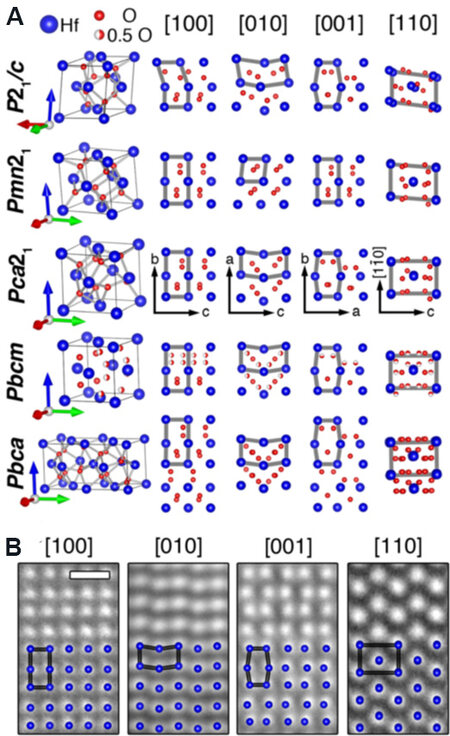
Figure 2. (A) HfO2 crystal structures for M-phase (P21/c), two non-centrosymmetric O-phases (Pmn21 and Pca21) and two centrosymmetric O-phases (Pbcm and Pbca) and their atom projections along four major zone axes. (B) STEM-HAADF images of
Recently, Luo et al.[99] provided evidence to distinguish these O-phases in Hf0.5Zr0.5O2 (HZO) thin films by directly mapping oxygen atoms using atomic-scale STEM-HAADF and STEM annular bright-field (STEM-ABF) techniques. Figure 3A-C show the sublattice of the Hf/Zr and O atoms projections along the [010] axis of HZO phases with different space groups. The O atom projections in the blank rectangle are different between the Pca21, Pbca and Pbcm phases. Figure 3D and E present atomic-resolution STEM-HADDF and STEM-ABF images of FE HZO films, respectively, in which the Hf/Zr and O atomic columns along the [010] axis match very well with the simulated results of the Pca21 phase.
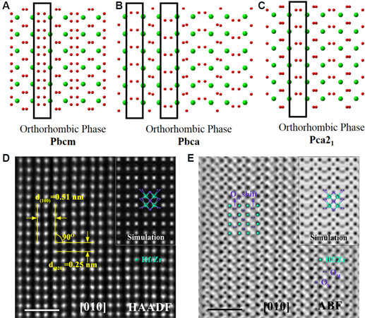
Figure 3. Projections of crystal structures of HfO2 with three O-phases along the [010] axis. The arrangements of O atoms in the black rectangles are different among (A) Pbcm, (B) Pbca and (C) Pca21. (D) STEM-HAADF image of HZO phase projected along [010] zone axis. Scale bar of 1 nm. (E) STEM-ABF image of (D) with the inset being a simulated ABF image. Scale bar is 1 nm[99]. STEM-HAADF: Scanning transmission electron microscopy-high angle annular dark-field; HZO: Hf0.5Zr0.5O2; ABF: annular bright-field.
With the exception of the Pca21structure, a rhombohedral phase (R-phase) with the R3m space group is also non-centrosymmetric. The R3m structure is obtained in epitaxial (111)HZO/(001) La0.7Sr0.3MnO3 (LSMO)/SrTiO3 (STO) substrates, as shown in Figure 4A and B. Devices based on this phase exhibit a large remanent polarization (Pr) of 34 μC·cm-2 and are free of a wake-up process. The R3m phase is only observed in epitaxial thin films, while the commonly reported Pca21phase can be found in both polycrystalline and epitaxial films. According to DFT calculations, the Pca21 phase has lower free energy than the R3m phase and is thus more stable and common in FE HfO2 films. However, epitaxial strain and size effects favor the R3m phase[29].
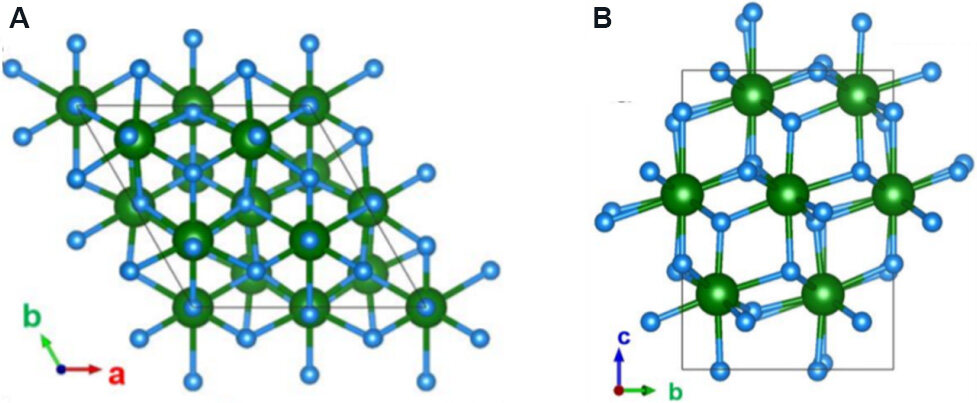
Figure 4. Polar R-phase (R3m) viewed from (A) the [001] axis and (B) the [100] axis of bulk HfO2 obtained by first-principles calculations. Hf and O atoms are represented by green and blue spheres, respectively[29].
FE HFO2 POLYCRYSTALLINE FILMS
In this section, various deposition methods for polycrystalline HfO2 films are reviewed, followed by the impact of the growth parameters on the FE phase and properties of HfO2 films, including dopants, film thickness and strain conditions. Finally, the phase transformation and FE properties under external stimuli, e.g., temperature and electric cycling, are also discussed.
Film deposition methods
The ALD method, which has been intensively studied for the semiconductor industry, has been widely used for the preparation of FE HfO2 films[16]. The precursors are commercially available materials for Hf, Si and Zr, e.g., tetrakis(ethylmethylamino)hafnium and HfCl4, tetrakis(dimethylamino)silane and SiCl4, and tetrakis(ethylmethylamino)zirconium. Ozone and water are used as oxygen sources while argon is used as a purge and carrier gas[19,20,52]. The initial HfO2 films deposited on TiN or TaN bottom electrodes are amorphous. A subsequent rapid thermal annealing for crystallization is applied after capping a top electrode layer to introduce ferroelectricity. A Pr of up to 35 μC·cm-2 and a coercive field (Ec) of up to 3.5 MV·cm-1 were experimentally achieved in ALD-based HfO2 films with various dopants, including Si, Zr, Y, La, Gd, Sr, Sc and N[23,53,75,100]. In addition, these ALD-based HfO2 films present a significant reduction of Pr with increasing film thickness and almost lose their ferroelectricity when the film thickness is over 20 nm[101]. There are some concerns regarding the practical application of the ALD method. First is the chemical reactions between a metal precursor, an oxygen source, a substrate or a previously deposited film, which makes it difficult to control the film processing parameters and leads to a narrow processing window[102]. In addition, sophisticated and high-cost facilities and the low deposition rate of ALD makes it less viable for practical manufacturing[21]. In order to solve these problems, other deposition methods, including physical vapor deposition (PVD), chemical solution deposition (CSD) and PLD have been explored[21,43]. A comparison of these methods is shown in Table 2[63,103-106].
| Method | Benefits | Drawbacks | Film structures |
| ALD | • Ease of subnanometer thickness control, good step coverage and large area uniformity • High conformality, e.g., 3D structures[103] • Widely used in CMOS technology in recent decades | • Slow deposition rates (100-300 nm/h) • Higher carbon contamination from metalorganic precursors • Narrow deposition temperature window • Moderate deposition temperature (~200 °C) and annealing (600-1000 °C) | • Polycrystalline films • Thermodynamic unpredicted phase transformation pathway: tetragonal-orthorhombic-monoclinic phase transition • Limited film thickness stabilizing the FE phase |
| PVD-PLD | • Nanometer thickness control • Enabling 3D integration • Controllable film morphology and stoichiometry by multiple process parameters, e.g., laser fluence, background pressure and substrate temperature • High deposition rate (~100 Å/min) • Cleanliness of the process due to the use of the laser (a filament is not required) • Numerous target materials, allowing the growth of complex oxides | • Complex mechanism • Ack-sputtering • Limited maximum area deposition by angular energy distribution | • Epitaxial films and polycrystalline films • Thermodynamically favored phase transformation pathway: monoclinic-orthorhombic phase transformation |
| PVD-sputtering | • Deposition at room temperature possible • Very high deposition rates and the associated low cost • Lower carbon contamination due to use of ceramic targets • Low annealing temperature of ~500-600 °C | • Dual targets are required for accurately controlling doping | • Polycrystalline films • Thick films up to 1 μm possessing ferroelectricity |
| CSD | • Cost-effectiveness, ease of use and high yield • Wide tunability with various dopant systems • Thicker FE films | • CSD precursors may be difficult to obtain • Resolution of layer thickness is poor • Nonuniform morphology |
For PVD methods, the sputtering, sputter power, atmosphere and deposition temperature can be precisely controlled to adjust HfO2 films with multiple phases with different phase fractions and the corresponding macroscopic FE performance. This not only benefits the exploration of the structure-property relationship of FE HfO2 films, but is also attractive for revealing how the growth parameters control the phases in obtained HfO2 films, especially the FE Pca21phase[107]. Mittmann et al.[108] prepared undoped HfO2 films using the sputtering method, in which the film thickness, annealing temperature and oxygen content were controllable. After annealing with temperatures higher than 600 °C, the films with thicknesses of 8-30 nm show a stable remanent polarization (Pr). For films with a thickness in the range of 8-20 nm, their Pr values increase with annealing temperature up to 1000 °C. For thicker films, 800 °C is the optimal anneal temperature. In addition, the concentration of oxygen (oxygen deficiency) within the HfO2 films is responsible for the stabilization of the O-phase by adjusting the nucleation of the nanocrystallite phase in the as-deposited films. The sputtering method is also promising for depositing HfO2 films at room temperature, because it can significantly change the kinetic energy of the sputtered films to control the phase types at room temperature without subsequent high-temperature processing[109]. The reduction of deposition temperature is always desirable for decreasing production costs and matching substrates that cannot sustain high temperatures, such as organic flexible substrates[110].
The CSD method is an inexpensive and flexible deposition technique with good adjustability of concentration and stoichiometry. Therefore, it is widely used for the deposition of FE and piezoelectric ceramic thin films[111,112]. Using the CSD method, Starschich et al.[43] successfully prepared Y:HfO2 films with a thickness of ~70 nm, which still possess Prover 13 μC·cm-2. The PLD method has been widely used to prepare highly oriented HfO2 films. Recently, 930-nm-thick 7%-Y:HfO2 films were deposited on (111)Pt/TiOx/SiO2/(001)Si substrates using this method. Interestingly, the resulting FE structures and properties were insensitive to the film thickness, which also makes HfO2 films attractive for structural characterization and piezoelectric applications[29,35,63].
Phase stability
The ferroelectricity in doped HfO2 films is attributed to the stabilization of the metastable non-centrosymmetric Pca21phase[32,38,99]. The FE phase Pca21 can be stabilized by various growth parameters during the film fabrication process with the above mentioned methods, i.e., ALD, PVD, CSD and PLD. The common growth parameters that can be controlled are doping (bulk free energy)[45,75,113,114], film thickness (grain size effect)[57,78,93] and capping layer (thermal strain)[16,115-117]. We will discuss how the polar Pca21phase is stabilized by these growth parameters. In addition, the ferroelectricity in HfO2 films has a strong electric field[118-121] and temperature dependence[18,122,123], which has a strong correlation with the phase transformation under external stimuli[25,122]. While previous reviews[51,82] focused mainly on the FE properties, we will summarize the microstructure-property relations.
Effects of dopants (bulk free energy)
The ferroelectricity in HfO2 films can be adjusted by dopant species. Various cations, including Si[16], Zr[74], Al[20], Y[19] and La[100,124], and an anion, N[114], have been incorporated into HfO2 films. All these dopants can induce ferroelectricity but have different doping sensitivity depending on the dopant size. For films with smaller sized dopants, such as Si and Al, macroscopic paraelectric (PE)-FE-antiferroelectric (AFE) transitions occur with increasing dopant concentration[16,18,20]. HfO2 films doped with Si were firstly reported to induce ferroelectricity and exhibited significant potential for industrial applications due to Si already being a standard element with mature technical parameters and contamination control methods[16]. In HfO2 films, Pr increases with a Si concentration of 2.6 to 3.1 mol.%. The AFE property gradually appears when the Si concentration is over 4.3 mol.%[16]. Similar results were observed in Al-doped HfO2 films. A robust FE behavior is achieved at an Al content of 4.8 mol.% and obvious AFE behavior occurs at an 8.5 mol.% Al content[20]. Zr is another promising dopant to maintain the FE properties in a wide Zr-content range because the Zr can substitute Hf in the whole composition range[125]. Figure 5A shows a polarization-electric field (P-E) hysteresis loop for the HZO films. The FE behavior in the HZO system is stabilized when the Zr concentration is 30-50 mol.%[62,74]. Figure 5B demonstrates how the ZrO2 content affects the Pr, dielectric constant (εr) and M-phase fraction in HfO2-ZrO2 solid solutions. The highest Pr is achieved at a 50 mol.% ZrO2 concentration, while the fraction of the M-phase (P21/c) decreases to 0% at this point. This result indicates that the centrosymmetric M-phase is suppressed with increasing doping concentration. The reduced M-phase promises the possibility of forming the non-centrosymmetric phase Pca21.
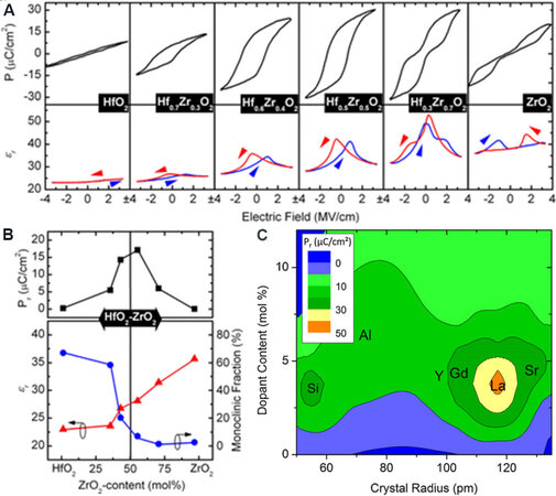
Figure 5. (A) P-E hysteresis at 1 kHz of 9-nm-thick HZO-based metal-insulator-metal capacitors. (B) Evolution of Pr, εr and M-phase fraction in the HfO2-ZrO2 solid solution with increasing ZrO2 content (mol.%)[74]. (C) Contour plot of Pr as a function of dopant radius and concentration[45]. HZO: Hf0.5Zr0.5O2; Pr: remanent polarization.
The doping sensitivity of various dopants is shown in Figure 5C[45]. Unlike small-sized dopants, large-sized dopants (e.g., Y, Gd and La) exhibit different PE-FE-PE transitions with increasing concentrations[19,21,124,126]. Müller et al.[19] prepared HfO2 films with Y concentrations varying from 2.3 to 12.3 mol.%. The highest Pr of 24 μC·cm-2 was achieved at a Y concentration of 5.2 mol.%. Unlike the AFE behavior in Si- or Al-doped HfO2 films, the HfO2 films with PMA (anneal for crystallization after top electrode deposition) and PDA (anneal for crystallization after top electrode deposition) change to paraelectric again when the concentration of Y increases to 12.3 mol.%, as shown in Figure 6.
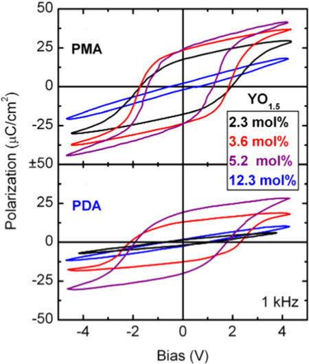
Figure 6. P-V hysteresis loops of 10 nm HfO2 films doped with Y from 2.3 to 12.3 mol.% treated with PMA and PDA processes[19].
To systematically investigate the dopant effects on phase types and ferroelectricity in HfO2 films, experiments and theoretical calculations were carried out with different dopant species (ionic size and valence) and concentrations. Schroeder et al.[45] compared the ferroelectricity of HfO2 films with various dopants of radii from 54 pm (Si) to 132 pm (Sr). AFE behavior (when T-phase occurs) occurred in HfO2 films with small-sized dopants, such as Si and Al, and this was attributed to the specific phase transformation path related to small dopants. For small dopants, like Si and Al, M-O-T-C phases transformations occur with increasing doping concentration[45]. On the contrary, M-O-C phase transformation takes place in HfO2 films with large dopants, such as Y, Gd, La and Sr, not favoring the formation of the T-phase that leads to AFE-like behavior. The T-phase contains four relatively short and four relatively long Hf-O bonds, which is more favorable with Si or Al doping because the short Si-O or
Later, more atoms (Al, Ga, Co, Ni, Mg, In, La, Y, Nd, Sm, Er, Sr and Ba) with different ionic radii (from 54 to 135 pm), valences and concentrations were incorporated in CSD-based HfO2 films[75]. The Prin HfO2 films with large dopants (from La to Sm, Pr≈ 14 μC·cm-2) is almost four times higher than that of small dopants (from Al to In, Pr ≈ 3.5 μC·cm-2). This is due to the promotion of the C-phase to O-phase transformation by the large dopants, with the assistance of oxygen vacancy movement under an applied electric field[75]. Similar results were also obtained in sputtered HfO2 films doped with Sc, Y, Nb, Al, Si, Ge and Zr[114]. Figures 7A and B show the switchable polarization (PSW) and the phase fractions of the O-, T- and C-phases as a function of doping species and concentration. Although these dopants show different doping sensitivities, the switchable polarization peaks remain at ~22 μC·cm-2. Meanwhile, the corresponding fractions of the O-, T- and C-phases increase to ~100% at high doping levels, indicating a phase transformation from the M-phase to the O-, T- and C-phases. Figures 7C and D show the relationships of
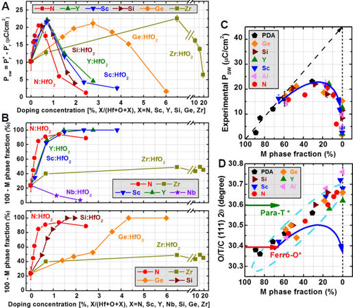
Figure 7. (A) Switchable polarization PSW of HfO2 films as a function of doping concentration for different dopants: Sc, Y, Si, Ge, Zr and N. (B) O-, T- and C-phase fraction of HfO2 films as a function of doping concentrations for various dopants. (C) PSW as a function of the M-phase fraction for HfO2 films with various dopants. (D) O-, T- and C-phase (111) peak positions as a function of the fraction of the M-phase for various dopants. The red and green arrows represent theoretical values for FE O-phase and non-FE T-phase, respectively[114]. PSW: switchable polarization; FE: ferroelectric.
In order to further understand the dopant effect on the stabilization of the Pca21 phase, first-principles calculations were carried out with 40 dopants by Batra et al.[113]. The results indicated a significant decrease in bulk free energy after doping with Ca, Sr, Ba, La, Y and Gd, although the Pca21phase could not be solely stabilized by any dopant. In addition, the Pca21 phase is more favored by dopants with large radii and low electronegativity due to the specific bonds between the dopant cation and the second nearest oxygen neighbor. Compared with divalent dopants, such as Ba and Sr, trivalent dopants, including La, Gd and Y, are considered to stabilize the polar Pca21phase at a lower lattice strain condition. These conclusions are consistent with the experimental results discussed above, illustrating that some dopants from rare earth metals (La, Gd and Y) to alkaline earth metals (Sr) show significant potential in enhancing the ferroelectricity in HfO2 films.
The understanding of the phase transformation with dopant concentration is interesting for both the fundamental understanding of HfO2 films and their applications. It is helpful to understand the origin of ferroelectricity in HfO2 films. In addition, the FE properties in HfO2 FEs can be manipulated by different dopants to optimize the device performance. For example, Park et al.[31] reported that the energy storage density was the highest in the Hf1-xZrxO2 system with x = 0.7. Doping is the most flexible method to tailor HfO2 FE thin films with the desired properties.
Effects of film thickness (surface energy)
According to the bulk free energy theory, the M-phase is more energetically favored compared to the FE Pca21phase that can be obtained in films with thicknesses of < 40 nm[16,19,52]. Park et al.[76] investigated the FE properties and the fraction of FE O-phase in Hf0.5Zr0.5O2 films with thicknesses from 10 to 25 nm. A consistent reduction of the Pr and O-phase fraction was found with increasing film thickness. Similar results were reported in undoped HfO2 films with thicknesses from 4 to 20 nm[93] [Figure 8A]. A reduction of Prand permittivity in the HfO2 films was observed when the film thickness increased from 6 to 20 nm. Grains in HfO2 films with thicknesses from 6 to 20 nm were characterized by TEM, as shown in Figure 8B. The individual grain grew across from bottom to top electrodes, in which the horizontal and vertical dimensions were of the same order of magnitude of film thickness. According to this result, a relation of grain size vs. film thickness was proposed, where the individual grain size in the HfO2 film depends on its vertical dimension, or in other words, the film thickness. Thus, a larger film thickness results in an enlarged grain size. As indicated by ab initio results, the FE O-phase with the Pca21 structure has a lower surface energy than the M-phase[57]. In the nanoscale HfO2 films, the existence of a large quantity of nanocrystal grains leads to a high surface-to-volume ratio. Therefore, the surface energy dominates the total Helmholtz free energy, leading to stabilization of the metastable Pca21phase that unfavored solely by the bulk free energy. In this case, the surface energy loses its dominant contribution to the total energy in thicker films and the obtained phase is mainly favored by the bulk free energy, resulting in stabilization of the M-phase.
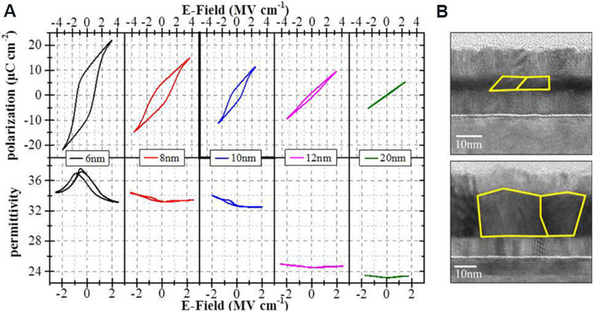
Figure 8. (A) Evolution of polarization-electric field and permittivity-electric field hysteresis with increasing thickness of undoped HfO2 thin films. (B) TEM micrograph of typical grains in 6 and 20 nm-thick HfO2 films[93]. TEM: Transmission electron microscopy.
Benefitting from their unusual size effect, HfO2 films can maintain spontaneous and switchable polarization, even for thicknesses down to 1 nm[129], unlike the scaling issues in perovskite FEs. This size effect in HfO2 FE films not only shifts the search for the fundamental limits from traditional perovskite FEs to next-generation fluorite structured oxides, but is also helpful for developing polarization-driven memories and ultrathin FE-based transistors.
In addition, contradictory reports are available in the literature on the effect of film thickness on Ec, even in epitaxial HfO2 films. Lyu et al.[130] reported that Ec decreases remarkably with film thickness in epitaxial HZO films, and the slope of the linear fit to log(Ec) vs. thickness is -0.61, which is consistent with the scaling value of -2/3 that is common in high quality perovskite FEs. A similar thickness-dependent Ecwas observed for epitaxial HZO films on Si(001)[69] and La-doped HZO films on STO(001) and Si(001)[131]. In contrast, the Ec was reported to remain almost constant with increasing film thickness in epitaxial Y-doped HfO2 films[132]. The microstructural origin for the different thickness-Ec relation is rarely reported. It was believed that microstructures would significantly affect the thickness and Ec relationship, which requires more work to reveal the role of microstructure.
Effects of capping electrodes and annealing (strain and quenching)
As-deposited HfO2 films from ALD normally consist of an amorphous structure. Crystallization by annealing should be carried out. In the annealing process, a capping layer is a significant promotion to induce ferroelectricity due to the strain effect (the strain is introduced by the different thermal expansion coefficients between the capping layer and the HfO2 film). Böscke et al.[16] reported that ferroelectricity only occurs in 10-nm-thick Si:HfO2 after annealing with a TiN top electrode capping. A more systematic investigation of Al:HfO2 films was conducted by Mueller et al.[20] on the FE properties in PMA samples with a TiN top capping layer [Pt/TiN(top)/Al:HfO2/TiN(bottom)/Si], and PDA samples without a TiN top capping layer. As shown in Figure 9, the PMA and PDA samples show similar PE-FE-AFE transitions with increasing doping concentration, but the Prof the PMA samples is always higher than that of the PDA samples.
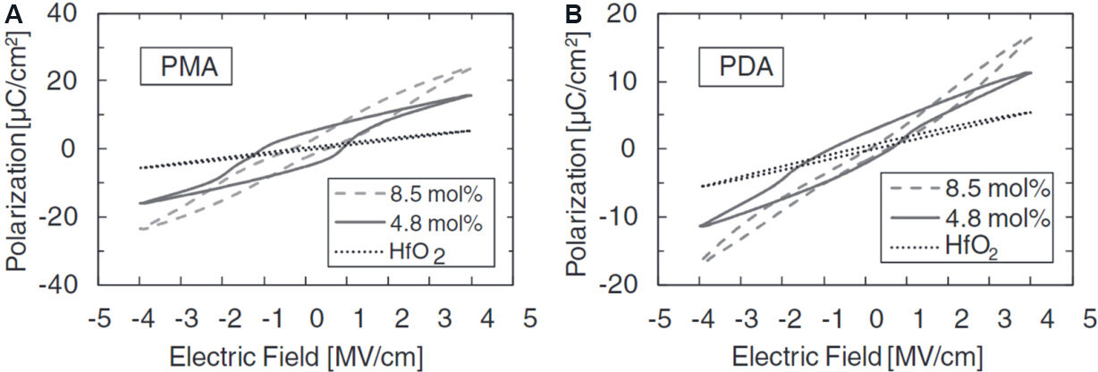
Figure 9. Polarization hysteresis for (A) PMA and (B) PDA samples[20].
Bottom electrodes also play a significant role in the ferroelectricity of HfO2 films, which can control the resulting grain orientations and produce in-plane lattice strain. Park et al.[115] clarified that grains in HZO/TiN (polycrystalline films/electrode) possess random orientations, while HfO2 films on (111)-oriented Pt bottom electrodes are (111)-textured. A high in-plane tensile strain larger than 1.5% is found in both types of films. For tetragonal grains with proper orientation [(110)-oriented], the transformation to the
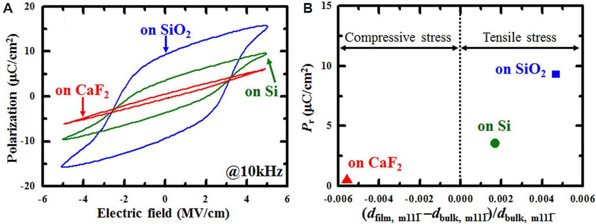
Figure 10. (A) P-E hysteresis of HZO thin films deposited on SiO2, Si and CaF2 substrates. (B) Relationship between remanent polarization and deviation of the lattice spacing[117]. HZO: Hf0.5Zr0.5O2.
Furthermore, other metal electrodes, such as W, Ru and Ir, have also been used for HfO2 FE fabrication to improve the endurance of the device or device integration ability[133-138]. Some field-induced behaviors, such as the wake-up effect and fatigue, are also related to the electrode properties[25,33].
FERROELECTRICITY AND MICROSTRUCTURAL EVOLUTION UNDER EXTERNAL STIMULI
Since FE HfO2 films are promising for memory devices and energy storage applications operating under repeated electric or thermal loading, the materials properties and corresponding device performance under external stimuli, such as temperature and electric field, must be considered. In this section, the phase transformations and FE device performance evolution under external stimuli in HfO2 films are reviewed.
Temperature
Temperature-dependent ferroelectricity is an interesting topic in FE HfO2 films. The FE-AFE transition with a temperature increase from 0 to 180 °C was first reported in 3.8 mol.% Si-doped HfO2 films by
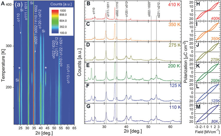
Figure 11. (A) An intensity contour map of GIXRD patterns of Si-doped HfO2 films from 110 to 410 K. GIXRD patterns of Si-doped HfO2 films measured at (B) 410, (C) 350, (D) 275, (E) 200, (F) 125 and (G) 110 K. P-E curves of Si-doped HfO2 films measured at (H) 400, (I) 350, (J) 275, (K) 200, (L) 125 and (M) 80 K[122]. GIXRD: Grazing incidence X-ray diffraction
Electric field
Although HfO2 FEs show significant potential for resolving critical difficulties that deter the commercialization of FE memories, they also suffer from remarkable instability issues induced by electric fields, namely, wake-up and fatigue[25,33,118,141]. A significant enhancement in ferroelectricity by electric field loading was first reported in Gd-doped HfO2 films by Mueller et al.[126]. Later, Zhou et al.[118] provided detailed experimental results in polarization change and identified it as the wake-up behavior in Si-doped HfO2 films. At the wake-up stage, Pr increases with electric cyclings and the two previously existing asymmetric coercive voltages tend to be symmetric. After the wake-up stage, the Prof HfO2 films show a degradation when the electric cycling continuously increases, leading to device failure (fatigue). Non-volatile FE memory devices are subjected to frequent read-out and write-in operation require robust stability. The electric field induced switching behaviors and phase transformation have side effects on device stability, thus their behaviors and the mechanism behind them should be understood for further device optimization.
The wake-up behavior is attributed to a transition of built-in bias. Pešić et al.[25] investigated some electrical parameters, including polarization, built-in bias and leakage current, which induce wake-up and fatigue, and concluded some trends during cyclic loadings. In the initial wake-up stage, the polarization increases while the built-in bias diminishes with a constant leakage current [Figure 12]. The constant leakage current indicates that no new defects form at this stage. Therefore, a possible origin for built-in bias is the evolution of the local defect (e.g., oxygen vacancies) distribution and/or phase transformation within a device. These oxygen vacancies are expected to occur at the interface between the TiN electrode and HfO2 films in the pristine HfO2 films, which induce the asymmetric distribution of the internal field that results in two peaks in the switching current curve [Figure 12B]. During the electric cycling process, these charged oxygen vacancies can move into the internal film under the electric field. The redistribution of oxygen vacancies improves the asymmetric internal field, which makes the two peaks (pristine state) in the switching current merge into one (wake-up state).
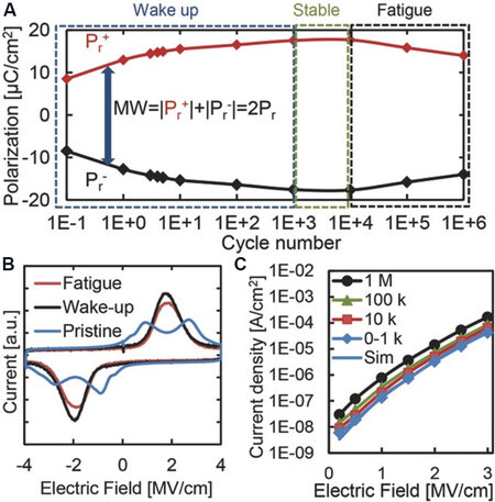
Figure 12. (A) Pr of Sr:HfO2 FE capacitors as a function of electric cyclings. (B) Current-voltage curves for the pristine, wake-up and fatigue stages. (C) Leakage current-electric field curves measured after different cycling numbers[25]. Pr: Remanent polarization; FE: ferroelectric.
In addition, a phase transformation is expected with increasing cyclic loadings. The bulk region undergoes an M-phase to O-phase transformation, while the interfacial region undergoes a T-phase to O-phase transformation, as confirmed by TEM characterization[25]. The field-induced phase changes at the wake-up stage were also observed by TEM in 10-nm-thick Si- and Gd-doped HfO2 films[33,119,142]. The O-, C- and T-phase to M-phase ratio is 0.2 for pristine films and increases to 1 after 1000 cycles, representing a phase transformation from the M-phase to the O-, C- and T-phases upon the electric cycle loadings, as shown in Figure 13A[33]. Similar phase transformations during the wake-up process were also observed by X-ray diffraction. Fields et al.[121] observed a decrease in the full width at half-maximum of the T- and O-phase superimposed peak, from 0.425 before the wake-up process to 0.406 after wake-up, which indicated the phase change from the T-phase to the O-phase during the wake-up process. A similar result was also reported in undoped and Y-doped HfO2 films by Nittayakasetwat and Kita[143].
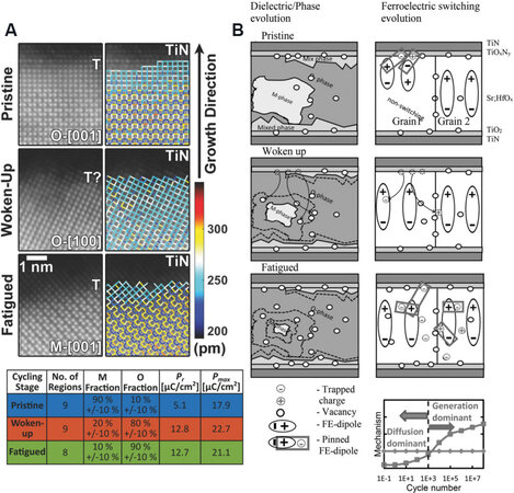
Figure 13. (A) STEM-HAADF images of HfO2 films at pristine, wake-up and fatigue stages, showing phase transformation and corresponding phase fractions at different stages[33]. (B) Proposed physical mechanism behind the field-induced FE behavior by coupling with phase transformation, defect generation and diffusion, and charge injection[25]. STEM-HAADF: Scanning transmission electron microscopy-high angle annular dark-field; FE: ferroelectric.
It is noteworthy that the redistribution of oxygen vacancies and the phase transformation during the wake-up process should not be considered separately. Previous experimental investigations indicate that the formation of the stable M-phase could be suppressed by an oxygen deficient atmosphere[62,102], while computational simulations suggest that the O-phase has a lower free energy with increasing oxygen vacancies[53]. Mittmann et al.[55] claimed that oxygen vacancies may act as nucleation sites for the polar phase, which promise a large number of nuclei that leads to a small average grain size during the crystallization process and therefore stabilizes the O-phase. During the wake-up process, oxygen vacancies can diffuse into the film interior easily at such a high electric field (in the order of MV cm-1), which may result in the phase transformation to the O-phase.
After the wake-up process, if the FE HfO2-based devices are applied with continuous electric cyclic loadings, these devices will reach the fatigue stage. At present, the reported field cycling endurance for devices based on polycrystalline La-doped HfO2 films[48] is no more than 1011. This value is much smaller than that of their perovskite counterparts (1015 for the MSP430 FR573x microcontroller, Texas Instruments[84]), making it a critical problem for HfO2-based devices. During the fatigue process, the leakage current increases, along with the reduction of polarization, which is attributed to the formation of new defects, e.g., Hf and O vacancies and their accumulation near grain boundaries. Pešić et al.[25] investigated the fatigue stage using dielectric-based simulation software and a commercial TCAD Sentaurus device simulator tool. The complete device stack is defined as TiN (top)/TiOxNy/TM-HfOx/FE-HfO2/TM-HfOx/TiOx/TiN (bottom), where TM-HfOx is the interfacial region consisting of a nonswitchable transitional material. In the fatigue stage, oxygen vacancies are generated at the electrode near the TiOx interface. The non-switchable regions, TM-HfOx, reduce the switching electric field for the FE layer and thus the number of switchable domains and polarization decrease.
Park et al.[84] discussed the limited endurance of FE HfO2 films and the possible affected factors on this phenomenon. They reported that both grain size and doping concentration influence the endurance property. In the case of polycrystalline FE HfO2 films, the FE O-phase is stabilized by the nanoscaled grain sizes in HfO2 films that result in significant grain boundaries for the accumulation of oxygen vacancies. Therefore, HfO2 films with larger grain sizes are expected to possess higher endurance, while the M-phase fraction also increases, resulting in a reduction in remanent polarization. In addition, the largest 2Pr of
Retention is another significant parameter for FE devices. FE HfO2 films can achieve retention times of up to a decade, which is higher than the retention time in perovskite FE materials, e.g., PZT [Pb(Zr,Ti)O3][69,144]. The high retention in HfO2 films is related to the reduced depolarization field/coercive field and trapping effects. Gong and Ma[144], Ma et al.[145] suggested that if the depolarization field is comparable to or smaller than Ec, the polarization decay for retention is low. In HfO2 FEs, the large Ecof ~1-2 MV cm-1 results in minimal polarization loss. In addition, the electron injection is induced by the remanent polarization during the device working, which is followed by electron trapping and then diminished polarization in the FE layer. In HfO2 FE films, the internal defects concentrations, e.g., grain boundaries, domain walls and point defects, are key to the polarization loss. Compared with perovskite FEs that have large thicknesses of ~100 nm, HfO2 films with thicknesses of ~10-40 nm possess robust ferroelectricity, in which the trap concentration is reduced by the thin film deposition.
As discussed above, the limited endurance and the long retention in HfO2 films are related to the very large Ecof ~1-2 MV cm-1, which is much higher than that of conventional perovskite FEs (~0.05 MV cm-1)[81]. Such a large Ecbrings both advantages and disadvantages to HfO2-based FE films. For example, HfO2 FE devices require a high driving voltage (≥ 3.0 V for 10-nm-thick films) to reach the saturated remnant polarization (2Pr) value due to the large Ec, and thus, degrades the device reliability during the endurance test. However, it improves the scalability of HfO2 film-based FeFET devices. The memory window (MW) of a FeFET is estimated as MW = 2Ec× t, where Ec is the coercive field and t is the thickness of the FE layer. From this aspect, the higher Ec is helpful to reduce the device dimensions. In addition, higher Ec can improve the retention of the FeFET of HfO2 films. This makes the Ec value attractive at a certain level.
This electric field-induced FE behavior is normally related to the phase transformation. However, the mechanism behind it is unclear. Pešić et al.[25] revealed that the existing defects, e.g., oxygen vacancies, can redistribute under the electric field, resulting in a phase transformation, as shown in Figure 13B. However, it is difficult to observe the direct evidence of defect redistribution under the electric field due to the present limitations of film quality and experimental techniques. Recently, FE domain switching behavior was observed due to the epitaxial rhombohedral (R-phase) HfO2 films with high single crystalline quality. Nukala et al.[146] showed the drift of oxygen vacancies across the HZO films between two LSMO electrodes by in-situ TEM with the integrated differential phase contrast (iDPC) mode. The oxygen vacancies move to the bottom electrode from the HZO films when the positive bias increases from 0 to 2 V. At a bias of 4 V, a phase transformation from the R-phase to M- and O-phases occurs [Figure 14]. It is noteworthy that the oxygen-reactive top LSMO electrode is the main source and sink of oxygen. This observation clarifies the microstructural origin of phase transformation from the R-phase to the O- and M-phases. However, this phase transformation path is not the most common one between the M- and O-phases. Therefore, further investigations should be carried out for FE HfO2 films with the O-phase with the Pca21 space group.
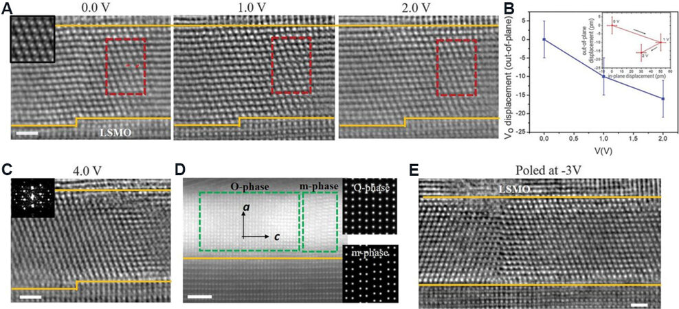
Figure 14. Oxygenation and deoxygenation of HZO and associated phase transformations. (A) STEM-iDPC images under increasing positive bias showing R-phase evolution of an HZO grain. (B) Out-of-plane displacement of VO with external bias in the marked supercell (red box) with respect to the positions in (A). Negative values indicate displacement toward bottom electrode. VO shows both in-plane and out-of-plane (toward bottom electrode) components (inset). (C) A new grain nucleates in the same region at +4 V, giving rise to a polycrystalline nature (FFT in inset). (D) Another region in HZO film back at 0 V showing the O- and M-phases. Note the change of orientation from [111] to [100]. (E) STEM-iDPC image of domains (mutually rotated by 180° about [111]) in R-phase, which is retained when poled at -3 V (imaged at 0 V). Scale bars: 1 nm in (A, C, E), 2 nm in (D). Interfaces between HZO and top and bottom LSMO are marked in orange[30]. HZO: Hf0.5Zr0.5O2; STEM-iDPC: scanning transmission electron microscopy-integrated differential phase contrast; LSMO: La0.7Sr0.3MnO3.
FE HfO2 EPITAXIAL FILMS
As discussed previously, polycrystalline HfO2 films have advantages in certain areas, including easy fabrication and CMOS compatibility for practical applications. However, some disadvantages hinder the practical application of these films. For example, problems related to the electric field induce wake-up and fatigue processes in HfO2 films, which significantly influence the device stability. The wake-up effect is attributed to the M- to O-phase transformation[33] and the fatigue may be induced by the accumulation of oxygen vacancies at grain boundaries in polycrystalline HfO2 films[121]. Epitaxial HfO2 films, possessing single-crystalline and boundary-free characteristics, are of significant interest in optimizing FE performance. This includes the elimination of the wake-up effect due to the phase transformation and extension of the device lifetime due to oxygen vacancy accumulation at grain boundaries. In addition, epitaxial HfO2 films can serve as a model system for physical mechanism investigations of new fluorite FE materials due to their single crystalline characteristics. In this section, the lattice matching relations between substrates and epitaxial HfO2 films are reviewed, followed by comparisons between polycrystalline and epitaxial HfO2 films in terms of their polarization, wake-up effect and fatigue behavior. Finally, some recent in-situ TEM observations of high-quality epitaxial films are reviewed.
FE phase stabilization in epitaxial HfO2 films
Epitaxial HfO2 films present single-crystalline structures with certain crystallographic orientations, benefiting both promoting FE properties and easing the investigation of fundamental issues due to their simple phase composition. Since the phase types and FE properties of epitaxial films are dominated by substrate types, here, epitaxial HfO2 films are reviewed according to substrate types. In addition, dopant concentration[63,147-152], film thickness[35,47,66,69,130,132,153-159] and process parameters, such as oxygen concentration[106,109,130,160] and annealing temperature[130,161], also have effects on FE phases in epitaxial HfO2 films. However, their effects are similar to those in polycrystalline films in terms of the microstructural mechanism, thus these parts are not discussed in this section.
Orthorhombic Y-doped HfO2 films on YSZ substrates
For epitaxial films, the initial film structure and final phase stability are determined by interfacial energy between substrates and HfO2 films. Normally, the interfacial energy of a coherent or a semi-coherent interface is relatively small, while the incoherent interface has much higher energy. Therefore, the FE O- and R-phases could also be stabilized with proper epitaxial relations.
YO1.5-doped HfO2 films were first epitaxially grown on (100) YSZ substrates using the PLD method by the group of Funakubo[63]. With increasing dopant concentration, the structure of the epitaxial HfO2 films changes from the non-FE M-phase to the FE O-phase, and finally to a high symmetric T-phase without ferroelectricity. Furthermore, the orientation of epitaxial orthorhombic YO1.5-HfO2 films could be adjusted by selecting appropriate substrates. In this case, the deposition temperature (700 °C) is higher than the Curie temperature (450 °C), resulting in the formation of a T-phase at this temperature[63]. During the cooling stage, high-temperature T-phase transforms to the O-phase. Since the c-axis (cT) is longer than the
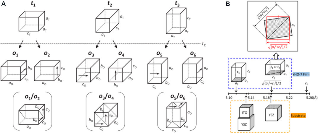
Figure 15. (A) Possible phase transformation paths from the T-phase to the O-phase. (B) Crystal parameter matching between HfO2 films and electrodes/substrates[162].
In Figure 15B, (001)-oriented (aT= 0.5115 nm) HfO2 films with the T-phase can be deposited on a (001)ITO (aITO= 0.5135 nm)//(001)YSZ substrate with a lattice mismatch of -0.39% and then transforms to the (100)-oriented O-phase. In addition, the (100)/(010)-oriented tetragonal HfO2 (sqrt [(aT2 + cT2)/2] = 0.5185 nm) films can be deposited on (001) YSZ (aYSZ= 0.5184 nm) by diagonal matching with lattice mismatch of 0.02% and then transforms to the (010)/(001) O-phase[162]. The thickness-dependent structure and FE performance of (111)-oriented epitaxial 0.07YO1.5-HfO2 (YHO7) films were investigated by
Orthorhombic HZO films on LSMO bottom electrode
LSMO has also been used as a bottom electrode and buffer layer for the epitaxial growth of HZO thin films because of the lattice matching and the consideration of interfacial chemistry[67]. LSMO layers were deposited on various oxide substrates with cubic or pseudocubic structures with lattice parameters in the range of 0.371 to 0.421 nm, resulting in different lattice mismatches for epitaxial (111)-oriented HZO films [d(111) = 0.298 nm > d(11-1)/(1-11)/(-111) = 0.294 nm] with different FE properties. The fraction of O-phase increases at larger substrate lattice parameters, indicating that this phase is more favored with tensile LSMO electrodes. A domain-matching mechanism is responsible for high-quality epitaxial HfO2 films in this (111)HZO//(001)LSMO system, although a structural dissimilarity and large lattice mismatch exist in this (111)HZO//(001)LSMO system, which is revealed by a STEM investigation, as shown in Figure 16[68].
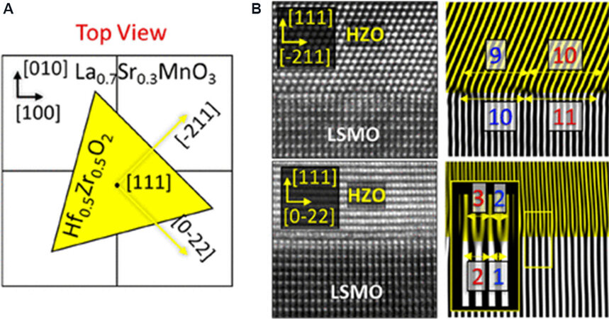
Figure 16. (A) Schematic top view of an HZO crystal on a LSMO(001) surface. (B) Cross-sectional STEM-HAADF image of HZO/LSMO heterostructure showing HZO crystal variants of the [$$\bar 2$$11] and [0$$\bar 1$$1] types. Reconstructed image from reflections in Fourier space corresponding to ($$\bar 1$$11) HZO and (110) LSMO planes. (inset) Fast Fourier transformation of both HZO and LSMO. Planes in the HZO layer are shown in yellow, while planes in the LSMO are given in white[68]. HZO: Hf0.5Zr0.5O2; LSMO: La0.7Sr0.3MnO3; STEM-HAADF: scanning transmission electron microscopy-high angle annular dark-field.
Rhombohedral HZO films on LSMO bottom electrodes
A new epitaxial rhombohedral (R3m) HZO thin film grown on a (001) La0.7Sr0.3MnO3/SrTiO3 (LSMO/STO) substrate was recently reported by Wei et al.[29]. Figure 17A presents a plan-view selected-area electron diffraction (SAED) pattern of a 9-nm-thick HZO film, showing 220 superposition spots from at least two domains (as shown in Figure 17C), with yellow and blue circles. The cross-sectional STEM-HAADF image of a 9-nm-thick HZO film in Figure 17B displays the coexistence of majority and minority HZO domains with [111]HZO and [001]HZO out-of-plane, respectively. In addition, from the fast Fourier transformation in Figure 17B, the estimated d111-HZO is around 2.953.01 Å. An interfacial HZO phase with a thickness of 2-3 monolayers is also found between the LSMO and HZO film, which is a (~8%) in-plane tensile strained T-phase (a = 3.60 Å in the unstrained T-phase and here, strained to the STO substrate, a = 3.91 Å), as shown in Figure 17D. A much lower out-of-plane parameter of c/2 = 2.31-2.44 Å is induced by the strained T-phase, leading to the generation of the R-phase under compressive strain (d111-r-HZO = 2.95-3.01 Å and d001-t-HZO = 2.31-2.44 Å). The obtained HZO film with the R-phase has a large FE polarization of up to 34 μC·cm-2 and no requirement for a wake-up stage.
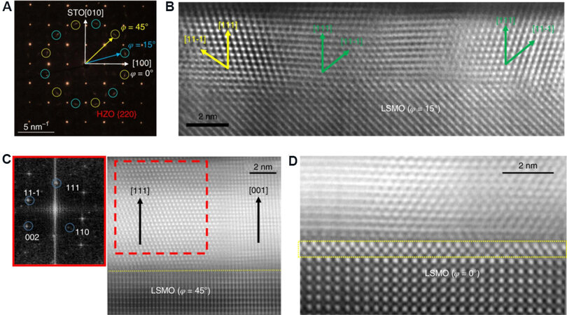
Figure 17. (A) Plan-view SAED pattern and (B) representative cross-sectional STEM-HAADF image of a 4-nm-thick film. (C) Cross-sectional STEM-HAADF image from a 9-nm-thick HZO sample. (D) STEM-HAADF image observed along STO [100] (the STO substrate is not shown in the images), revealing an interfacial T-phase layer of HZO[29]. SAED: Selected-area electron diffraction; STEM-HAADF: scanning transmission electron microscopy-high angle annular dark-field; HZO: Hf0.5Zr0.5O2; STO: SrTiO3.
A systematic investigation for the strain-induced stabilization of the R-phase was carried out by
It can be concluded that the phase formation (orthorhombic or rhombohedral) in epitaxial HZO films depends on various factors, including the epitaxial strain and interfacial chemistry. The underlying mechanisms and accurate control for epitaxial phase require further exploration in future works.
Epitaxial HfO2 films on silicon
Lee et al.[163] reported that (001)-oriented Y-doped HfO2 films were epitaxially grown on (001)Si with YSZ as the buffer layer. The O-phase Pca21 with the out-of-plane direction of [001]/[010] is illustrated by X-ray
Comparison of FE properties between polycrystalline and epitaxial HfO2 films
In polycrystalline HfO2 films, the FE O-phase coexists with non-FE T-, M- and C-phases. Therefore, the reduction of Pr is induced by the generation of non-polar phases from polar phases. Under an electric field, the non-polar phases transform to a polar phase, resulting in a higher Pr value, known as the wake-up effect[118]. In addition, oxygen vacancies accumulate along grain boundaries during the electric cycling loading, leading to large remanent leakage current and retention loss, known as device fatigue[25]. Epitaxial methods are used to obtain HfO2 films with a single O-phase, reducing the fraction of non-polar phases and grain boundaries that are detrimental for device performance. Therefore, improvements in remanent polarization, wake-up stage, and fatigue are expected in epitaxial films, as shown in
Comparison of FE properties between polycrystalline and epitaxial HfO2 films
| Material | Film type | Deposition | Top/bottom electrodes | Substrates | Temperature (°C) | Thickness (nm) | Phase type | Pr (μC·cm-2) | Ec (MV·cm-1) | Endurance cycles | Ref. |
| 7 mol.%-YO1.5-HfO2 | Epitaxial | PLD | Pt/ITO | (001)YSZ | RT + 1000 °C annealing | ~15 | (001)-O phase | > 25 | 2-3 | / | 2018[165] |
| Polycrystal | PLD | / | (001)Si | RT + 1000 °C annealing | ~15 | Poly-O phase | ~17 | 1.45 | / | 2019[35] | |
| 5.2 mol.%-YO1.5-HfO2 | Polycrystal | ALD | TiN | Si | RT + 600 °C annealing | ~10 | Poly-O phase | 24 | ~1.2 | / | 2011[19] |
| Hf0.5Zr0.5O2 | Epitaxial | PLD | LSMO | (001)STO | 800 °C | 5 | (111)-R phase | 34 | ~5 | / | 2018[29] |
| Hf0.5Zr0.5O2 | Epitaxial | PLD | Pt/LSMO | YSZ/(001)Si | 800 °C | 4.6 | (111)-O phase | 33 | ~4 | 1 × 10¹¹ | 2020[69] |
| Hf0.5Zr0.5O2 | Polycrystal | ALD | TiN | Si | 250 + 400 °C annealing | 10 | Poly-O phase | 25.45 | ~1 | / | 2018[50] |
| Hf0.5Zr0.5O2 | Polycrystal | ALD | TiN | (100)Si | 175 + 500 °C annealing | 5.1 | Poly-O phase | 4.1 | / | 1 × 10¹⁰ | 2018[166] |
| Hf0.42Zr0.58O2 | Polycrystal | PA-AOD | TiN/Ge | (100)Ge | 225 + 750 °C annealing | 13 | Poly-O phase | 34.4 | 1.8 | 1 × 10⁵ | 2019[125] |
| Hf0.5Zr0.49La0.01O2 | Epitaxial | PLD | Pt/LSMO | (001)STO | 800 °C | 4.8 | (111)-O phase | ~20 | ~3.7 | 5 × 10¹⁰ | 2020[131] |
| Hf0.5Zr0.49La0.01O2 | Epitaxial | PLD | Pt/LSMO | (001)STO | 800 °C | 6.3 | (111)-O phase | ~30 | ~3.5 | 1 × 10⁹ | 2020[131] |
| 0.7 mol.%-La:(Hf, Zr)O2 | Polycrystal | ALD | TiN | Si | 235 + 500 °C annealing | 10 | Poly-O phase | 14.5 | / | 1011 | 2019[48] |
| 1 mol.%-La:(Hf, Zr)O2 | Polycrystal | PAALD | TiN | Si | 235 + 400 °C annealing | 10 | Poly-O phase | ~15 | 0.8 | 4 × 10¹⁰ | 2018[167] |
| 3-4 mol.%-La:HfO2 | Polycrystal | ALD | TiN | Si | 225 + 650 °C annealing | 9 | Poly-O phase | 40 | 1.2 | / | 2014[45] |
For HfO2 epitaxial films, the highest polarization value is 34 μC·cm-2 in (111)-oriented rhombohedral
Up to now, epitaxial HfO2 films are less investigated than their polycrystalline counterparts. It is much more difficult to grow epitaxial films with a single phase and certain orientations than polycrystalline films because of the requirements of lattice matching between a film and its substrate. The first epitaxial HfO2 film was reported in 2015, based on an ITO coated YSZ substrate and a PLD method. In addition, polycrystalline HfO2 films are mainly based on the ALD technique that is a mature fabrication method, while the epitaxial HfO2 is mainly prepared by PLD that is relatively less popular at present. However, the excellent FE performance has been demonstrated within epitaxial HfO2 films. At present, epitaxial films have been to the research core, more investigations will be carried for optimizing FE performance and proposing fundamental mechanisms related to phase stability and fatigue behavior.
CONCLUSIONS, CHALLENGES AND PERSPECTIVES
In conclusion, the discovery of ferroelectricity in fluorite-structure HfO2 films has both commercial potentials and fundamental research meanings as next-generation FE devices. Since HfO2 films have promising CMOS compatibility and high scalability, they will attract increasing interest for future memory devices. The inspiring development will encourage more explorations of new FE materials, such as nano-scale amorphous Al2O3 that is promising for non-volatile field-effect transistors[168]. In addition, the discovered ferroelectricity in this new-type fluorite material and nanoscale films triggered significant interest in fundamental investigations. Some results have been obtained. For example, the unexpected ferroelectricity in HfO2 films is attributed to the non-centrosymmetric O-phase Pca21 or R-phase R3m. These phases are metastable but can be stabilized by various growth parameters, e.g., dopants, film thickness and interfacial strain. In addition, FE HfO2 films exhibit PE-FE-AFE/PE evolution under external stimuli (temperature and bias). In particular, the Prof HfO2 ferroelectrics increases with electric cycles during the wake-up stage, followed by a decrease to a low value until device failure at the fatigue stage, leading to significant stability concerns for practical electronic devices. These two stages are related to the complicated interplay between phases transformation, defects redistribution and generation, and charge injection, significantly affecting the device stability and lifetime.
As discussed in this review, the FE properties and microstructural evolution under external stimuli are determined by film microstructures. Thus, a clear understanding of the microstructural transformation is a vital step for optimizing the FE properties of HfO2 devices. Electron microscopy is a powerful tool to give atomic-level structural information. It has made a great contribution to these fundamental issues in HfO2 films, e.g., characterization of FE phase, nanoscale grain morphology and interfacial regions between HfO2 films and electrodes. However, there are still some important issues rely on the thorough investigation of microstructures.
First is the impact of dopants on the microstructure transformation. In the present research, it is clear that the FE phases and FE properties can be adjusted by the dopants. But how does it happen? The general mechanism of the dopant effect is not clear yet. Understanding this issue can give a guideline for ferroelectrics design with suitable FE or AFE properties. However, there is a complicated coupling interplay among phase transformation, defects, and dopants. Generally, defects in HfO2 films are adjusted by dopants, and then both of them influence the phase transformation, the determined relations among them should be clarified. It is quite difficult to directly observe the defect migration without reliable characterization tools. Fortunately, the state-of-the-art STEM and spectroscopy techniques, including annular bright field imaging, high-angle annular dark-field imaging, (integrated) differential phase-contrast imaging, and electron energy loss spectroscopy techniques provide unique opportunities to directly precisely map the structural and elemental information of both the dopant elements and matrix elements in atomic scale[59,169-173]. Heavy and light elements can be detected and displayed simultaneously, providing a full spectrum of visualizing the microstructures-properties relationship. In the future, these techniques will be powerful tools for further investigation of the relationship between microstructures and FE properties.
Another important issue regarding HfO2 films is their FE property evolution with external stimuli, e.g., wake-up and fatigue. For electronic devices, repeatable device operation with bias voltage is required. The instability problems, such as wake-up and fatigue, should be suppressed. Therefore, the mechanism, especially the microstructural origin, behind these phenomena should be clarified. In-situ electron microscopy, including heating[174], biasing[30,175], straining[176,177] and their combinations, in a STEM/TEM have been very powerful in understanding the dynamic and kinetic behavior of FE materials. Phase transformation, oxygen octahedral tilting, defect migration, domain evolution under separate/combined biasing, straining and heating environments could be captured and analyzed in real-time. The recorded high spatial, temporal, and energy resolution of the recording information from state-of-the-art in-situ electron microscopy opens a new door to address these critical questions in FE HfO2 material systems.
DECLARATIONS
Authors’ contributionsMade the literature review and drafted the original version: Zhao D
Revised the manuscript: Chen Z, Liao X
Conceived and supervised the project: Chen Z, Liao X
Availability of data and materialsNot applicable.
Financial support and sponsorshipThis project is supported by the Australian Research Council Discovery Project DP190101155.
Conflicts of interestAll authors declared that there are no conflicts of interest.
Ethical approval and consent to participateNot applicable.
Consent for publicationNot applicable.
Copyright© The Author(s) 2022.
REFERENCES
1. Bowen CR, Kim HA, Weaver PM, Dunn S. Piezoelectric and ferroelectric materials and structures for energy harvesting applications. Energy Environ Sci 2014;7:25-44.
2. Wang Y, Ganpule C, Liu BT, et al. Epitaxial ferroelectric Pb(Zr, Ti)O3 thin films on Si using SrTiO3 template layers. Appl Phys Lett 2002;80:97-9.
3. Grigoriev A, Do DH, Kim DM, et al. Nanosecond domain wall dynamics in ferroelectric Pb(Zr, Ti)O(3) thin films. Phys Rev Lett 2006;96:187601.
4. Jia CL, Urban KW, Alexe M, Hesse D, Vrejoiu I. Direct observation of continuous electric dipole rotation in flux-closure domains in ferroelectric Pb(Zr,Ti)O3. Science 2011;331:1420-3.
5. Wang T, Jin L, Li C, Hu Q, Wei X, Lupascu D. Relaxor ferroelectric BaTiO3-Bi(Mg2/3Nb1/3)O3 ceramics for energy storage application. J Am Ceram Soc 2015;98:559-66.
6. Merz WJ. Switching time in ferroelectric BaTiO3 and its dependence on crystal thickness. J Appl Phys 1956;27:938-43.
7. Bellaiche L, Vanderbilt D. Intrinsic piezoelectric response in perovskite alloys: PMN-PT versus PZT. Phys Rev Lett 1999;83:1347-50.
8. Hwang GT, Park H, Lee JH, et al. Self-powered cardiac pacemaker enabled by flexible single crystalline PMN-PT piezoelectric energy harvester. Adv Mater 2014;26:4880-7.
9. Xu S, Yeh YW, Poirier G, McAlpine MC, Register RA, Yao N. Flexible piezoelectric PMN-PT nanowire-based nanocomposite and device. Nano Lett 2013;13:2393-8.
10. Izyumskaya N, Alivov Y, Cho S, Morkoç H, Lee H, Kang Y. Processing, structure, properties, and applications of PZT thin films. Crit Rev Solid State Mater Sci 2007;32:111-202.
11. Khan AI, Keshavarzi A, Datta S. The future of ferroelectric field-effect transistor technology. Nat Electron 2020;3:588-97.
12. Monga S, Tomar S, Vilarinho PM, Singh A. Effect of substrates on optical properties of ferroelectric PZT (52/48) thin films. Mater Today Proc 2021;36:616-20.
13. Long P, Chen C, Pang D, Liu X, Yi Z. Optical, electrical, and photoelectric properties of nitrogen-doped perovskite ferroelectric BaTiO 3 ceramics. J Am Ceram Soc 2019;102:1741-7.
14. Shvartsman VV, Lupascu DC, Green DJ. Lead-free relaxor ferroelectrics. J Am Ceram Soc 2012;95:1-26.
15. Cartier E, Kerber A, Ando, T, et al. . Fundamental aspects of HfO2-based high-k metal gate stack reliability and implications on tinv-scaling. 2011 International Electron Devices Meeting; 2011 Dec 5-7; Washington, DC, USA. IEEE; 2011. p. 18.4.1-18.4.4.
16. Böscke TS, Müller J, Bräuhaus D, Schröder U, Böttger U. Ferroelectricity in hafnium oxide thin films. Appl Phys Lett 2011;99:102903.
17. Böscke TS, Müller J, Bräuhaus D, Schröder U, Böttger U. . Ferroelectricity in hafnium oxide: CMOS compatible ferroelectric field effect transistors. 2011 International Electron Devices Meeting; 2011 Dec 5-7; Washington, DC, USA. IEEE; 2011. p. 24.5.1-24.5.4.
18. Böscke TS, Teichert S, Bräuhaus D, et al. Phase transitions in ferroelectric silicon doped hafnium oxide. Appl Phys Lett 2011;99:112904.
19. Müller J, Schröder U, Böscke TS, et al. Ferroelectricity in yttrium-doped hafnium oxide. J Appl Phys 2011;110:114113.
20. Mueller S, Mueller J, Singh A, et al. Incipient ferroelectricity in Al-doped HfO2 thin films. Adv Funct Mater 2012;22:2412-7.
21. Olsen T, Schröder U, Müller S, et al. Co-sputtering yttrium into hafnium oxide thin films to produce ferroelectric properties. Appl Phys Lett 2012;101:082905.
22. Schenk T, Schroeder U, Pešić M, Popovici M, Pershin YV, Mikolajick T. Electric field cycling behavior of ferroelectric hafnium oxide. ACS Appl Mater Interfaces 2014;6:19744-51.
23. Hoffmann M, Schroeder U, Künneth C, et al. Ferroelectric phase transitions in nanoscale HfO2 films enable giant pyroelectric energy conversion and highly efficient supercapacitors. Nano Energy 2015;18:154-64.
24. Hoffmann M, Pešić M, Chatterjee K, et al. Direct observation of negative capacitance in polycrystalline ferroelectric HfO2. Adv Funct Mater 2016;26:8643-9.
25. Pešić M, Fengler FPG, Larcher L, et al. Physical mechanisms behind the field-cycling behavior of HfO2-based ferroelectric capacitors. Adv Funct Mater 2016;26:4601-12.
26. Park MH, Schenk T, Hoffmann M, et al. Effect of acceptor doping on phase transitions of HfO2 thin films for energy-related applications. Nano Energy 2017;36:381-9.
27. Baumgarten L, Szyjka T, Mittmann T, et al. Impact of vacancies and impurities on ferroelectricity in PVD- and ALD-grown HfO2 films. Appl Phys Lett 2021;118:032903.
29. Wei Y, Nukala P, Salverda M, et al. A rhombohedral ferroelectric phase in epitaxially strained Hf0.5Zr0.5O2 thin films. Nat Mater 2018;17:1095-100.
30. Nukala P, Ahmadi M, Wei Y, et al. Reversible oxygen migration and phase transitions in hafnia-based ferroelectric devices. Science 2021;372:630-5.
31. Park MH, Kim HJ, Kim YJ, Moon T, Kim KD, Hwang CS. Thin HfxZr1-xO2 films: a new lead-free system for electrostatic supercapacitors with large energy storage density and robust thermal stability. Adv Energy Mater 2014;4:1400610.
32. Sang X, Grimley ED, Schenk T, Schroeder U, Lebeau JM. On the structural origins of ferroelectricity in HfO2 thin films. Appl Phys Lett 2015;106:162905.
33. Grimley ED, Schenk T, Sang X, et al. Structural changes underlying field-cycling phenomena in ferroelectric HfO2 thin films. Adv Electron Mater 2016;2:1600173.
34. Xu X, Huang FT, Qi Y, et al. Kinetically stabilized ferroelectricity in bulk single-crystalline HfO2:Y. Nat Mater 2021;20:826-32.
35. Mimura T, Shimizu T, Funakubo H. Ferroelectricity in YO1.5-HfO2 films around 1 μm in thickness. Appl Phys Lett 2019;115:032901.
36. Müller J, Polakowski P, Mueller S, Mikolajick T. Ferroelectric hafnium oxide based materials and devices: assessment of current status and future prospects. ECS J Solid State Sci Technol 2015;4:N30-5.
37. Clima S, Wouters DJ, Adelmann C, et al. Identification of the ferroelectric switching process and dopant-dependent switching properties in orthorhombic HfO2: a first principles insight. Appl Phys Lett 2014;104:092906.
38. Huan TD, Sharma V, Rossetti GA, Ramprasad R. Pathways towards ferroelectricity in hafnia. Phys Rev B 2014:90.
39. Falkowski M, Künneth C, Materlik R, Kersch A. Unexpectedly large energy variations from dopant interactions in ferroelectric HfO2 from high-throughput ab initio calculations. npj Comput Mater 2018:4.
40. Lee HJ, Lee M, Lee K, et al. Scale-free ferroelectricity induced by flat phonon bands in HfO2. Science 2020;369:1343-7.
41. Qi Y, Singh S, Lau C, et al. Stabilization of competing ferroelectric phases of HfO_{2} under epitaxial strain. Phys Rev Lett 2020;125:257603.
42. Cheynet MC, Pokrant S, Tichelaar FD, Rouvière J. Crystal structure and band gap determination of HfO2 thin films. J Appl Phys 2007;101:054101.
43. Starschich S, Griesche D, Schneller T, Waser R, Böttger U. Chemical solution deposition of ferroelectric yttrium-doped hafnium oxide films on platinum electrodes. Appl Phys Lett 2014;104:202903.
44. Mulaosmanovic H, Ocker J, Müller S, et al. Switching kinetics in nanoscale hafnium oxide based ferroelectric field-effect transistors. ACS Appl Mater Interfaces 2017;9:3792-8.
45. Schroeder U, Yurchuk E, Müller J, et al. Impact of different dopants on the switching properties of ferroelectric hafniumoxide. Jpn J Appl Phys 2014;53:08LE02.
46. Das D, Gaddam V, Jeon S. Demonstration of high ferroelectricity (Pr ~ 29 μC/cm2) in Zr rich HfxZr1-xO2 films. IEEE Electron Device Lett 2020;41:34-7.
47. Kim SJ, Mohan J, Lee J, et al. Effect of film thickness on the ferroelectric and dielectric properties of low-temperature (400 °C)
48. Kozodaev MG, Chernikova AG, Korostylev EV, et al. Mitigating wakeup effect and improving endurance of ferroelectric HfO2-ZrO2 thin films by careful La-doping. J Appl Phys 2019;125:034101.
49. Lyu X, Si M, Shrestha PR, et al. . Record fast polarization switching observed in ferroelectric hafnium oxide crossbar arrays. 2020 IEEE Silicon Nanoelectronics Workshop (SNW); 2020 Jun 13-14; Honolulu, HI, USA. IEEE; 2020. p. 7-8.
50. Yurchuk E, Müller J, Knebel S, et al. Impact of layer thickness on the ferroelectric behaviour of silicon doped hafnium oxide thin films. Thin Solid Films 2013;533:88-92.
51. Park MH, Lee YH, Kim HJ, et al. Ferroelectricity and antiferroelectricity of doped thin HfO2-based films. Adv Mater 2015;27:1811-31.
52. Müller J, Böscke TS, Bräuhaus D, et al. Ferroelectric Zr0.5Hf0.5O2 thin films for nonvolatile memory applications. Appl Phys Lett 2011;99:112901.
53. Hoffmann M, Schroeder U, Schenk T, et al. Stabilizing the ferroelectric phase in doped hafnium oxide. J Appl Phys 2015;118:072006.
54. Starschich S, Menzel S, Böttger U. Evidence for oxygen vacancies movement during wake-up in ferroelectric hafnium oxide. Appl Phys Lett 2016;108:032903.
55. Mittmann T, Michailow M, Lomenzo PD, et al. Stabilizing the ferroelectric phase in HfO2-based films sputtered from ceramic targets under ambient oxygen. Nanoscale 2021;13:912-21.
56. Materano M, Mittmann T, Lomenzo PD, et al. Influence of oxygen content on the structure and reliability of ferroelectric
57. Materlik R, Künneth C, Kersch A. The origin of ferroelectricity in Hf1-xZrxO2: a computational investigation and a surface energy model. J Appl Phys 2015;117:134109.
58. Ding W, Zhang Y, Tao L, Yang Q, Zhou Y. The atomic-scale domain wall structure and motion in HfO2-based ferroelectrics: a first-principle study. Acta Materialia 2020;196:556-64.
60. Chen Z, Wang X, Ringer SP, Liao X. Manipulation of nanoscale domain switching using an electron beam with omnidirectional electric field distribution. Phys Rev Lett 2016;117:027601.
61. Chen Z, Hong L, Wang F, et al. Facilitation of ferroelectric switching via mechanical manipulation of hierarchical nanoscale domain structures. Phys Rev Lett 2017;118:017601.
62. Park MH, Lee DH, Yang K, et al. Review of defect chemistry in fluorite-structure ferroelectrics for future electronic devices. J Mater Chem C 2020;8:10526-50.
63. Shimizu T, Katayama K, Kiguchi T, Akama A, Konno TJ, Funakubo H. Growth of epitaxial orthorhombic YO1.5-substituted HfO2 thin film. Appl Phys Lett 2015;107:032910.
64. Shimizu T, Katayama K, Kiguchi T, et al. The demonstration of significant ferroelectricity in epitaxial Y-doped HfO2 film. Sci Rep 2016;6:32931.
65. Lyu J, Fina I, Fontcuberta J, Sánchez F. Epitaxial integration on Si(001) of ferroelectric Hf0.5Zr0.5O2 capacitors with high retention and endurance. ACS Appl Mater Interfaces 2019;11:6224-9.
66. Zhang Z, Hsu SL, Stoica VA, et al. Epitaxial ferroelectric Hf0.5Zr0.5O2 with metallic pyrochlore oxide electrodes. Adv Mater 2021;33:e2006089.
67. Estandía S, Dix N, Gazquez J, et al. Engineering ferroelectric Hf0.5Zr0.5O2 thin films by epitaxial stress. ACS Appl Electron Mater 2019;1:1449-57.
68. Estandía S, Dix N, Chisholm MF, Fina I, Sánchez F. Domain-matching epitaxy of ferroelectric Hf0.5Zr0.5O2 (111) on La2/3Sr1/3MnO3 (001). Crystal Growth & Design 2020;20:3801-6.
69. Lyu J, Song T, Fina I, Sánchez F. High polarization, endurance and retention in sub-5 nm Hf0.5Zr0.5O2 films. Nanoscale 2020;12:11280-7.
70. Lyu J, Fina I, Bachelet R, et al. Enhanced ferroelectricity in epitaxial Hf0.5Zr0.5O2 thin films integrated with Si(001) using SrTiO3 templates. Appl Phys Lett 2019;114:222901.
71. Jesse S, Rodriguez BJ, Choudhury S, et al. Direct imaging of the spatial and energy distribution of nucleation centres in ferroelectric materials. Nat Mater 2008;7:209-15.
72. Arlt G. The influence of microstructure on the properties of ferroelectric ceramics. Ferroelectrics 1990;104:217-27.
73. Wu H, Zhang Y, Wu J, Wang J, Pennycook SJ. Microstructural origins of high piezoelectric performance: a pathway to practical lead-free materials. Adv Funct Mater 2019;29:1902911.
74. Müller J, Böscke TS, Schröder U, et al. Ferroelectricity in simple binary ZrO2 and HfO2. Nano Lett 2012;12:4318-23.
75. Starschich S, Boettger U. An extensive study of the influence of dopants on the ferroelectric properties of HfO2. J Mater Chem C 2017;5:333-8.
76. Park M, Joon Kim H, Jin Kim Y, Lee W, Moon T, Seong Hwang C. Evolution of phases and ferroelectric properties of thin Hf0.5Zr0.5O2 films according to the thickness and annealing temperature. Appl Phys Lett 2013;102:242905.
77. Park MH, Kim HJ, Kim YJ, et al. Study on the size effect in Hf0.5Zr0.5O2 films thinner than 8 nm before and after wake-up field cycling. Appl Phys Lett 2015;107:192907.
78. Batra R, Tran HD, Ramprasad R. Stabilization of metastable phases in hafnia owing to surface energy effects. Appl Phys Lett 2016;108:172902.
79. Nukala P, Wei Y, de Haas V, Guo Q, Antoja-lleonart J, Noheda B. Guidelines for the stabilization of a polar rhombohedral phase in epitaxial Hf0.5Zr0.5O2 thin films. Ferroelectrics 2020;569:148-63.
80. Estandía S, Gàzquez J, Varela M, et al. Critical effect of the bottom electrode on the ferroelectricity of epitaxial Hf0.5Zr0.5O2 thin films. J Mater Chem C 2021;9:3486-92.
81. Hwang CS. Prospective of semiconductor memory devices: from memory system to materials. Adv Electron Mater 2015;1:1400056.
82. Fan Z, Chen J, Wang J. Ferroelectric HfO2-based materials for next-generation ferroelectric memories. J Adv Dielect 2016;06:1630003.
83. Schroeder U, Slesazeck S, Mikolajick T. . Nonvolatile field-effect transistors using ferroelectric doped HfO2 films. In: Park B, Ishiwara H, Okuyama M, Sakai S, Yoon S, editors. Ferroelectric-gate field effect transistor memories. Dordrecht: Springer Netherlands; 2016. p. 57-72.
84. Park MH, Lee YH, Mikolajick T, Schroeder U, Hwang CS. Review and perspective on ferroelectric HfO2-based thin films for memory applications. MRS Communications 2018;8:795-808.
85. Kim SJ, Mohan J, Summerfelt SR, Kim J. Ferroelectric Hf0.5Zr0.5O2 thin films: a review of recent advances. JOM 2019;71:246-55.
86. Ali F, Zhou D, Sun N, et al. Fluorite-structured ferroelectric-/antiferroelectric-based electrostatic nanocapacitors for energy storage applications. ACS Appl Energy Mater 2020;3:6036-55.
87. Cao J, Shi S, Zhu Y, Chen J. An overview of ferroelectric hafnia and epitaxial growth. Phys Status Solidi RRL 2021;15:2100025.
88. Fina I, Sánchez F. Epitaxial ferroelectric HfO2 films: growth, properties, and devices. ACS Appl Electron Mater 2021;3:1530-49.
89. Materano M, Lomenzo PD, Kersch A, Park MH, Mikolajick T, Schroeder U. Interplay between oxygen defects and dopants: effect on structure and performance of HfO2-based ferroelectrics. Inorg Chem Front 2021;8:2650-72.
90. Curtis CE, Doney LM, Johnson JR. Some properties of hafnium oxide, hafnium silicate, calcium hafnate, and hafnium carbide. J American Ceramic Society 1954;37:458-65.
91. Tang J, Kai M, Kobayashi Y, et al. . A high-pressure high-temperature X ray study of phase relations and polymorphism of HfO2. In: Manghnani MH, Yagi T, editors. Properties of Earth and Planetary Materials at High Pressure and Temperature. Washington: American Geophysical Union; 1998. p. 401-7.
92. Ohtaka O, Fukui H, Kunisada T, et al. Phase relations and volume changes of hafnia under high pressure and high temperature. J Am Ceram Soc 2001;84:1369-73.
93. Polakowski P, Müller J. Ferroelectricity in undoped hafnium oxide. Appl Phys Lett 2015;106:232905.
94. Pal A, Narasimhan VK, Weeks S, Littau K, Pramanik D, Chiang T. Enhancing ferroelectricity in dopant-free hafnium oxide. Appl Phys Lett 2017;110:022903.
95. Luo J, Zhang H, Wang Z, et al. Improvement of ferroelectric properties in undoped hafnium oxide thin films using thermal atomic layer deposition. Jpn J Appl Phys 2019;58:SDDE07.
96. Ruh R, Corfield PWR. Crystal structure of monoclinic hafnia and comparison with monoclinic zirconia. J Am Ceram Soc 1970;53:126-9.
98. Adams DM, Leonard S, Russell DR, Cernik RJ. X-ray diffraction study of Hafnia under high pressure using synchrotron radiation. J Phys Condens Matter 1991;52:1181-6.
99. Luo Q, Cheng Y, Yang J, et al. A highly CMOS compatible hafnia-based ferroelectric diode. Nat Commun 2020;11:1391.
100. Kozodaev MG, Chernikova AG, Korostylev EV, et al. Ferroelectric properties of lightly doped La:HfO2 thin films grown by plasma-assisted atomic layer deposition. Appl Phys Lett 2017;111:132903.
101. Park MH, Lee YH, Kim HJ, et al. Surface and grain boundary energy as the key enabler of ferroelectricity in nanoscale hafnia-zirconia: a comparison of model and experiment. Nanoscale 2017;9:9973-86.
102. Lee YH, Kim HJ, Moon T, et al. Preparation and characterization of ferroelectric Hf0.5Zr0.5O2 thin films grown by reactive sputtering. Nanotechnology 2017;28:305703.
103. Hsain HA, Lee Y, Materano M, et al. Many routes to ferroelectric HfO2: a review of current deposition methods. Journal of Vacuum Science & Technology A 2022;40:010803.
104. Starschich S, Griesche D, Schneller T, Böttger U. Chemical solution deposition of ferroelectric hafnium oxide for future lead free ferroelectric devices. ECS J Solid State Sci Technol 2015;4:P419-23.
105. Shimura R, Mimura T, Shimizu T, Tanaka Y, Inoue Y, Funakubo H. Preparation of near-1-µm-thick {100}-oriented epitaxial Y-doped HfO2 ferroelectric films on (100)Si substrates by a radio-frequency magnetron sputtering method. J Ceram Soc Japan 2020;128:539-43.
106. Suzuki T, Shimizu T, Mimura T, Uchida H, Funakubo H. Epitaxial ferroelectric Y-doped HfO2 film grown by the RF magnetron sputtering. Jpn J Appl Phys 2018;57:11UF15.
107. Reichelt K, Jiang X. The preparation of thin films by physical vapour deposition methods. Thin Solid Films 1990;191:91-126.
108. Mittmann T, Materano M, Lomenzo PD, et al. Origin of ferroelectric phase in undoped HfO2 films deposited by sputtering. Adv Mater Interfaces 2019;6:1900024.
109. Mimura T, Shimizu T, Uchida H, Funakubo H. Room-temperature deposition of ferroelectric HfO2-based films by the sputtering method. Appl Phys Lett 2020;116:062901.
110. Bretos I, Jiménez R, Wu A, Kingon AI, Vilarinho PM, Calzada ML. Activated solutions enabling low-temperature processing of functional ferroelectric oxides for flexible electronics. Adv Mater 2014;26:1405-9.
112. Hodes G. . Chemical solution deposition of semiconductor films. 1st ed. New York: CRC press; 2002.
113. Batra R, Huan TD, Rossetti GA, Ramprasad R. Dopants promoting ferroelectricity in hafnia: insights from a comprehensive chemical space exploration. Chem Mater 2017;29:9102-9.
114. Xu L, Nishimura T, Shibayama S, Yajima T, Migita S, Toriumi A. Kinetic pathway of the ferroelectric phase formation in doped HfO2 films. J Appl Phys 2017;122:124104.
115. Park M, Joon Kim H, Jin Kim Y, Moon T, Seong Hwang C. The effects of crystallographic orientation and strain of thin Hf0.5Zr0.5O2 film on its ferroelectricity. Appl Phys Lett 2014;104:072901.
116. Lomenzo PD, Takmeel Q, Zhou C, et al. TaN interface properties and electric field cycling effects on ferroelectric Si-doped HfO2 thin films. J Appl Phys 2015;117:134105.
117. Shiraishi T, Katayama K, Yokouchi T, et al. Impact of mechanical stress on ferroelectricity in (Hf0.5Zr0.5)O2 thin films. Appl Phys Lett 2016;108:262904.
118. Zhou D, Xu J, Li Q, et al. Wake-up effects in Si-doped hafnium oxide ferroelectric thin films. Appl Phys Lett 2013;103:192904.
119. Chouprik A, Zakharchenko S, Spiridonov M, et al. Ferroelectricity in Hf0.5Zr0.5O2 thin films: a microscopic study of the polarization switching phenomenon and field-induced phase transformations. ACS Appl Mater Interfaces 2018;10:8818-26.
120. Fengler F, Park MH, Schenk T, Pešić M, Schroeder U. . Field cycling behavior of ferroelectric HfO2-based capacitors. Ferroelectricity in doped hafnium oxide: materials, properties and devices. Elsevier; 2019. p. 381-98.
121. Fields SS, Smith SW, Ryan PJ, et al. Phase-exchange-driven wake-up and fatigue in ferroelectric hafnium zirconium oxide films. ACS Appl Mater Interfaces 2020;12:26577-85.
122. Park MH, Chung C, Schenk T, et al. Origin of temperature-dependent ferroelectricity in Si-doped HfO2. Adv Electron Mater 2018;4:1700489.
123. Mimura T, Shimizu T, Sakata O, Funakubo H. Large thermal hysteresis of ferroelectric transition in HfO2-based ferroelectric films. Appl Phys Lett 2021;118:112903.
124. Schroeder U, Richter C, Park MH, et al. Lanthanum-doped hafnium oxide: a robust ferroelectric material. Inorg Chem 2018;57:2752-65.
125. Zacharaki C, Tsipas P, Chaitoglou S, et al. Very large remanent polarization in ferroelectric Hf1-xZrxO2 grown on Ge substrates by plasma assisted atomic oxygen deposition. Appl Phys Lett 2019;114:112901.
126. Mueller S, Adelmann C, Singh A, Van Elshocht S, Schroeder U, Mikolajick T. Ferroelectricity in Gd-doped HfO2 thin films. ECS J Solid State Sci Technol 2012;1:N123-6.
127. Fischer D, Kersch A. Stabilization of the high-k tetragonal phase in HfO2: the influence of dopants and temperature from ab initio simulations. J Appl Phys 2008;104:084104.
128. Lee C, Cho E, Lee H, Hwang CS, Han S. First-principles study on doping and phase stability of HfO2. Phys Rev B 2008;78:012102.
129. Cheema SS, Kwon D, Shanker N, et al. Enhanced ferroelectricity in ultrathin films grown directly on silicon. Nature 2020;580:478-82.
130. Lyu J, Fina I, Solanas R, Fontcuberta J, Sánchez F. Growth window of ferroelectric epitaxial Hf0.5Zr0.5O2 thin films. ACS Appl Electron Mater 2019;1:220-8.
131. Song T, Bachelet R, Saint-girons G, Solanas R, Fina I, Sánchez F. Epitaxial ferroelectric la-doped Hf0.5Zr0.5O2 thin films. ACS Appl Electron Mater 2020;2:3221-32.
132. Mimura T, Shimizu T, Uchida H, Sakata O, Funakubo H. Thickness-dependent crystal structure and electric properties of epitaxial ferroelectric Y2O3-HfO2 films. Appl Phys Lett 2018;113:102901.
133. Karbasian G, dos Reis R, Yadav AK, Tan AJ, Hu C, Salahuddin S. Stabilization of ferroelectric phase in tungsten capped Hf0.8Zr0.2O2. Appl Phys Lett 2017;111:022907.
134. Lin Y, Mcguire F, Franklin AD. Realizing ferroelectric Hf0.5Zr0.5O2 with elemental capping layers. Journal of Vacuum Science & Technology 2018;36:011204.
135. Cao R, Liu Q, Liu M, et al. Improvement of endurance in HZO-based ferroelectric capacitor using Ru electrode. IEEE Electron Device Lett 2019;40:1744-7.
136. Onaya T, Nabatame T, Sawamoto N, et al. Improvement in ferroelectricity of HfxZr1-xO2 thin films using top- and bottom-ZrO2 nucleation layers. APL Materials 2019;7:061107.
137. Kim H, Kashir A, Oh S, Hwang H. A new approach to achieving strong ferroelectric properties in TiN/Hf0.5Zr0.5O2/TiN devices. Nanotechnology 2021;32:055703.
138. Wang D, Zhang Y, Wang J, et al. Enhanced ferroelectric polarization with less wake-up effect and improved endurance of Hf0.5Zr0.5O2 thin films by implementing W electrode. J Mater Sci Mater Med 2022;104:1-7.
139. Park MH, Kim HJ, Kim YJ, Moon T, Kim KD, Hwang CS. Toward a multifunctional monolithic device based on pyroelectricity and the electrocaloric effect of thin antiferroelectric HfxZr1-xO2 films. Nano Energy 2015;12:131-40.
140. Ali F, Zhou D, Ali M, et al. Recent progress on energy-related applications of HfO2-based ferroelectric and antiferroelectric materials. ACS Appl Electron Mater 2020;2:2301-17.
141. Lee TY, Lee K, Lim HH, et al. Ferroelectric polarization-switching dynamics and wake-up effect in Si-doped HfO2. ACS Appl Mater Interfaces 2019;11:3142-9.
142. Martin D, Müller J, Schenk T, et al. Ferroelectricity in Si-doped HfO2 revealed: a binary lead-free ferroelectric. Adv Mater 2014;26:8198-202.
143. Nittayakasetwat S, Kita K. Evidence of ferroelectric HfO2 phase transformation induced by electric field cycling observed at a macroscopic scale. Solid-State Electronics 2021;184:108086.
144. Gong N, Ma T. Why is FE-HfO2 more suitable than PZT or SBT for scaled nonvolatile 1-T memory cell? IEEE Electron Device Lett 2016;37:1123-6.
145. Ma TP, Gong N. . Retention and endurance of FeFET memory cells. 2019 IEEE 11th International Memory Workshop (IMW); 2019 May 12-15; Monterey, CA, USA. IEEE; 2019. p. 1-4.
146. Nukala P, Ahmadi M, Wei Y, et al. Operando observation of reversible oxygen migration and phase transitions in ferroelectric devices. Available from: https://arxiv.org/ftp/arxiv/papers/2010/2010.10849.pdf [Last accessed on 22 Feb 2022].
147. Song T, Tan H, Dix N, et al. Stabilization of the ferroelectric phase in epitaxial Hf1-xZrxO2 enabling coexistence of ferroelectric and enhanced piezoelectric properties. ACS Appl Electron Mater 2021;3:2106-13.
148. Shimizu T, Katayama K, Funakubo H. Epitaxial growth of YO1.5 doped HfO2 films on (100) YSZ substrates with various concentrations. Ferroelectrics 2017;512:105-10.
149. Shiraishi T, Choi S, Kiguchi T, et al. Fabrication of ferroelectric Fe doped HfO2 epitaxial thin films by ion-beam sputtering method and their characterization. Jpn J Appl Phys 2018;57:11UF02.
150. Nukala P, Antoja-Lleonart J, Wei Y, Yedra L, Dkhil B, Noheda B. Direct epitaxial growth of polar (1-x)HfO2-(x)ZrO2 ultrathin films on silicon. ACS Appl Electron Mater 2019;1:2585-93.
151. Shiraishi T, Choi S, Kiguchi T, Shimizu T, Funakubo H, Konno TJ. Formation of the orthorhombic phase in CeO2-HfO2 solid solution epitaxial thin films and their ferroelectric properties. Appl Phys Lett 2019;114:232902.
152. Song T, Tan H, Bachelet R, Saint-Girons G, Fina I, Sánchez F. Impact of La concentration on ferroelectricity of La-doped HfO2 epitaxial thin films. ACS Appl Electron Mater 2021;3:4809-16.
153. Liu W, Liu M, Zhang R, Ma R, Wang H. Thickness-modulated anisotropic ferromagnetism in Fe-doped epitaxial HfO2 thin films. Appl Phys Lett 2017;111:172404.
154. Li T, Zhang N, Sun Z, et al. Epitaxial ferroelectric Hf0.5Zr0.5O2 thin film on a buffered YSZ substrate through interface reaction. J Mater Chem C 2018;6:9224-31.
155. Lyu J, Fina I, Solanas R, Fontcuberta J, Sánchez F. Robust ferroelectricity in epitaxial Hf1/2Zr1/2O2 thin films. Appl Phys Lett 2018;113:082902.
156. Li T, Ye M, Sun Z, et al. Origin of ferroelectricity in epitaxial Si-doped HfO2 films. ACS Appl Mater Interfaces 2019;11:4139-44.
157. Mimura T, Shimizu T, Katsuya Y, Sakata O, Funakubo H. Thickness- and orientation-dependences of Curie temperature in ferroelectric epitaxial Y doped HfO 2 films. Jpn J Appl Phys 2020;59:SGGB04.
158. Zhang Y, Yang Q, Tao L, Tsymbal EY, Alexandrov V. Effects of strain and film thickness on the stability of the rhombohedral phase of HfO2. Phys Rev Applied 2020;14:014068.
159. Song T, Bachelet R, Saint-girons G, Dix N, Fina I, Sánchez F. Thickness effect on the ferroelectric properties of La-doped HfO2 epitaxial films down to 4.5 nm. J Mater Chem C 2021;9:12224-30.
160. Song T, Solanas R, Qian M, Fina I, Sánchez F. Large enhancement of ferroelectric polarization in Hf0.5Zr0.5O2 films by low plasma energy pulsed laser deposition. J Mater Chem C 2022;10:1084-9.
161. Mimura T, Shimizu T, Kiguchi T, et al. Effects of heat treatment and in situ high-temperature X-ray diffraction study on the formation of ferroelectric epitaxial Y-doped HfO2 film. Jpn J Appl Phys 2019;58:SBBB09.
162. Katayama K, Shimizu T, Sakata O, et al. Orientation control and domain structure analysis of {100}-oriented epitaxial ferroelectric orthorhombic HfO2-based thin films. J Appl Phys 2016;119:134101.
163. Lee K, Lee TY, Yang SM, Lee DH, Park J, Chae SC. Ferroelectricity in epitaxial Y-doped HfO2 thin film integrated on Si substrate. Appl Phys Lett 2018;112:202901.
164. Bégon-lours L, Mulder M, Nukala P, et al. Stabilization of phase-pure rhombohedral HfZrO4 in pulsed laser deposited thin films. Phys Rev Materials 2020:4.
165. Shimizu T, Mimura T, Kiguchi T, et al. Ferroelectricity mediated by ferroelastic domain switching in HfO2-based epitaxial thin films. Appl Phys Lett 2018;113:212901.
166. Walters G, Shekhawat A, Rudawski NG, Moghaddam S, Nishida T. Tiered deposition of sub-5 nm ferroelectric Hf1-xZrxO2 films on metal and semiconductor substrates. Appl Phys Lett 2018;112:192901.
167. Chernikova AG, Kozodaev MG, Negrov DV, et al. Improved ferroelectric switching endurance of La-doped Hf0.5Zr0.5O2 thin films. ACS Appl Mater Interfaces 2018;10:2701-8.
168. Peng Y, Zhang G, Xiao W, et al. Ferroelectric-like non-volatile FET with amorphous gate insulator for supervised learning applications. IEEE J Electron Devices Soc 2021;9:1145-50.
169. Jia CL, Mi SB, Urban K, Vrejoiu I, Alexe M, Hesse D. Atomic-scale study of electric dipoles near charged and uncharged domain walls in ferroelectric films. Nat Mater 2008;7:57-61.
170. Jia CL, Nagarajan V, He JQ, et al. Unit-cell scale mapping of ferroelectricity and tetragonality in epitaxial ultrathin ferroelectric films. Nat Mater 2007;6:64-9.
171. Jia CL, Lentzen M, Urban K. Atomic-resolution imaging of oxygen in perovskite ceramics. Science 2003;299:870-3.
172. Jia CL, Thust A, Urban K. Atomic-scale analysis of the oxygen configuration at a SrTiO3 dislocation core. Phys Rev Lett 2005;95:225506.
173. Chen Z, Li F, Huang Q, et al. Giant tuning of ferroelectricity in single crystals by thickness engineering. Sci Adv 2020;6:eabc7156.
174. Nukala P, Ahmadi M, Antoja-lleonart J, et al. In situ heating studies on temperature-induced phase transitions in epitaxial Hf0.5Zr0.5O2/La0.67Sr0.33MnO3 heterostructures. Appl Phys Lett 2021;118:062901.
175. Huang Q, Chen Z, Cabral MJ, et al. Direct observation of nanoscale dynamics of ferroelectric degradation. Nat Commun 2021;12:2095.
176. Chen Z, Hong L, Wang F, et al. Kinetics of domain switching by mechanical and electrical stimulation in relaxor-based ferroelectrics. Phys Rev Applied 2017:8.
Cite This Article
Export citation file: BibTeX | RIS
OAE Style
Zhao D, Chen Z, Liao X. Microstructural evolution and ferroelectricity in HfO2 films. Microstructures 2022;2:2022007. http://dx.doi.org/10.20517/microstructures.2021.11
AMA Style
Zhao D, Chen Z, Liao X. Microstructural evolution and ferroelectricity in HfO2 films. Microstructures. 2022; 2(2): 2022007. http://dx.doi.org/10.20517/microstructures.2021.11
Chicago/Turabian Style
Zhao, Dou, Zibin Chen, Xiaozhou Liao. 2022. "Microstructural evolution and ferroelectricity in HfO2 films" Microstructures. 2, no.2: 2022007. http://dx.doi.org/10.20517/microstructures.2021.11
ACS Style
Zhao, D.; Chen Z.; Liao X. Microstructural evolution and ferroelectricity in HfO2 films. Microstructures. 2022, 2, 2022007. http://dx.doi.org/10.20517/microstructures.2021.11
About This Article
Copyright

Data & Comments
Data


 Cite This Article 44 clicks

 Like This Article 16
likes
Like This Article 16
likes


Comments
Comments must be written in English. Spam, offensive content, impersonation, and private information will not be permitted. If any comment is reported and identified as inappropriate content by OAE staff, the comment will be removed without notice. If you have any queries or need any help, please contact us at support@oaepublish.com.